

Switching regulator
- Summary
- Abstract
- Description
- Claims
- Application Information
AI Technical Summary
Benefits of technology
Problems solved by technology
Method used
Image

Examples
first embodiment
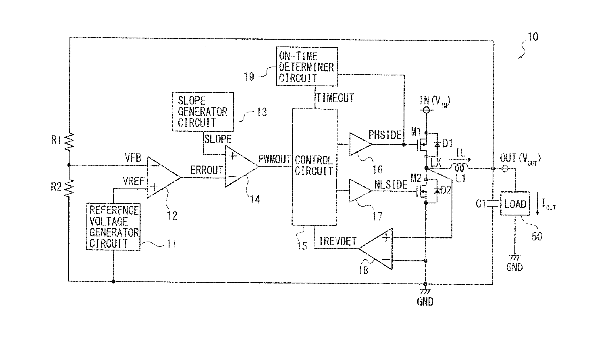
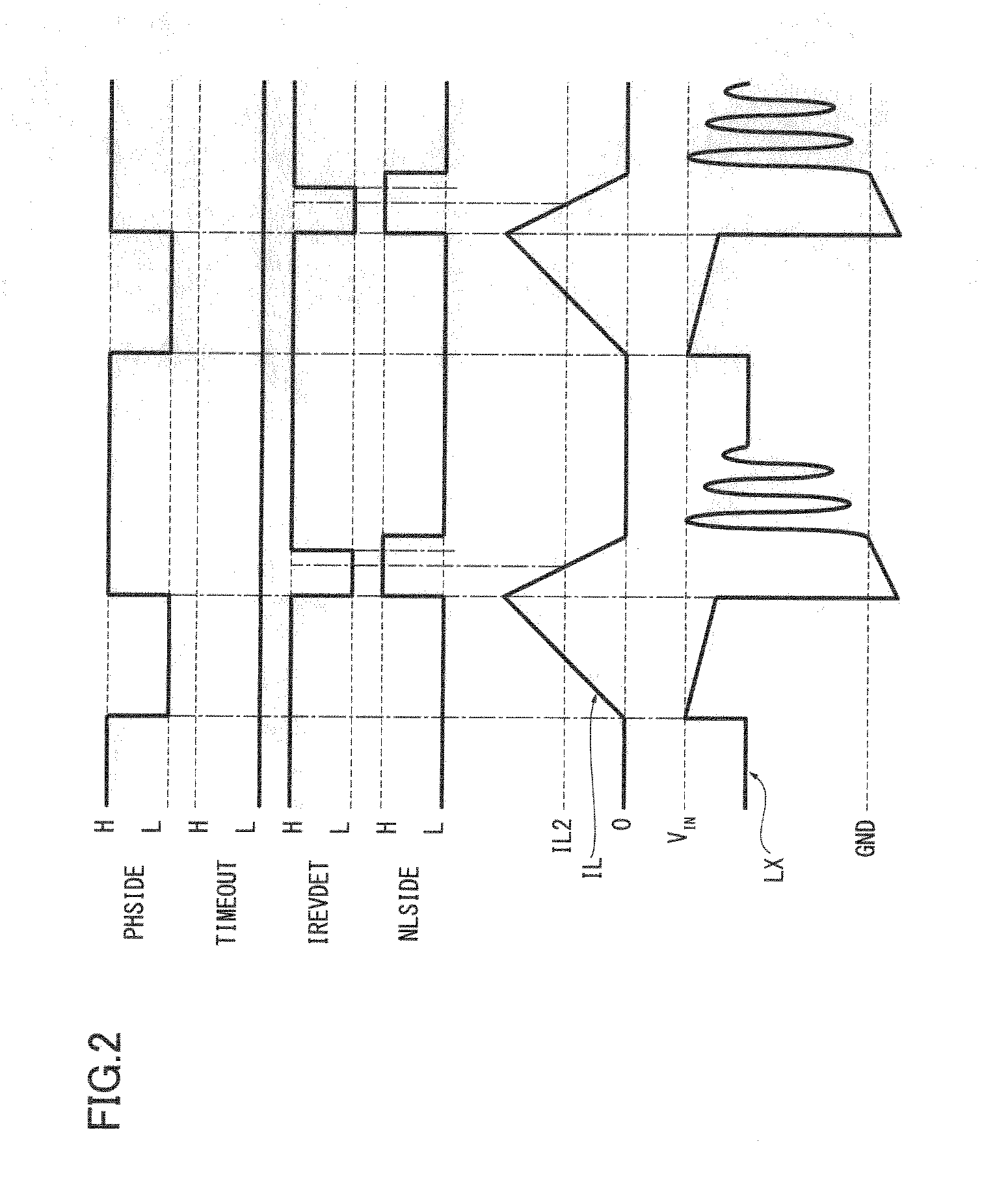
[0029]The structure of a switching regulator according to the first embodiment is described referring to FIG. 1. The switching regulator is a synchronous rectifier type configured to receive an input voltage VIN at an input terminal IN, convert it to a certain constant voltage and output it as an output voltage VOUT from an output terminal OUT to a load 50.
[0030]The switching regulator 10 comprises a first switching transistor M1 as a first switching element and a second switching transistor M2 as a second switching element. The first and second switching transistors M1, M2 are paired to conduct switching operation for output control over the input voltage VIN. By switching by the first and second switching transistors M1, M2, the input voltage VIN to the input terminal IN is converted to a certain constant output voltage and output from the output terminal OUT as the output voltage VOUT.
[0031]The first switching transistor M1 comprises a PMOS transistor and operates by a gate signa...
second embodiment
[0084]Next, a switching regulator 102 according to a second embodiment is described referring to FIGS. 7 to 9. The switching regulator 102 comprises an inductor current comparator 21 instead of the on-time determiner circuit 19 of the switching regulator 10 according to the first embodiment and its basic structure is the same as that of the switching regulator 10. Therefore, a detailed description thereof is omitted. FIG. 7 shows the structure of the switching regulator 102. FIG. 8 is a timing chart showing a variation (waveform) in the signals of the switching regulator 102 when a difference between input voltage VIN and output voltage VOUT is not small. FIG. 9 is a timing chart showing a variation (waveform) in the signals of the switching regulator 102 when a difference between input voltage VIN and output voltage VOUT is small.
[0085]The switching regulator 102 comprises the inductor current comparator 21 as an operation monitor in place of the on-time determiner circuit 19. The ...
third embodiment
[0111]Next, a switching regulator 10 according to a third embodiment is described referring to FIGS. 10 to 12. The switching regulator 103 is different from the switching regulator 10 in the first embodiment in that it additionally comprises an on-time setting circuit 22 and its basic structure is the same as that of the switching regulator 10. FIG. 10 shows the structure of the switching regulator 103. FIG. 11 is a timing chart showing a variation (waveform) in the signals of the switching regulator 103 when a difference between input voltage VIN and output voltage VOUT is not small. FIG. 12 is a timing chart showing a variation (waveform) in the signals of the switching regulator 103 when a difference between input voltage VIN and output voltage VOUT is small.
[0112]The switching regulator 103 additionally includes the on-time setting circuit 22 to set an ON time T2 for which the ON state of the second switching transistor M2 is maintained. The on-time setting circuit 22 is connect...
PUM
 Abstract
Description
Claims
Application Information