Method of etching a boron doped carbon hardmask

a technology of boron doped carbon hardmask and pattern, which is applied in the direction of basic electric elements, electrical discharge tubes, electrical apparatus, etc., can solve the problems of increasing processing capabilities, increasing the difficulty of deep etching high aspect ratio (har) features, and increasing the difficulty of etching patterns in the current conventional amorphous carbon hardmask layer without generating

Inactive Publication Date: 2015-03-05
APPLIED MATERIALS INC
View PDF6 Cites 43 Cited by
  • Summary
  • Abstract
  • Description
  • Claims
  • Application Information

AI Technical Summary

Benefits of technology

[0010]In another embodiment, a method for etching a boron doped hardmask layer is provided that includes flowing a process gas comprising CH4, Cl2, SF6 and O2 into a processing chamber, forming a plasma in the processing chamber from the process gas, and etchin

Problems solved by technology

However, with the continued miniaturization of circuit technology, the dimensions of the size and pitch of circuit features, such as interconnects, have placed additional demands on processing capabilities.
As device feature sizes become smaller, it has become increasingly more difficult to etch a pattern in the current conventional amorphous carbon hardmask layers without generating defects in the pattern lines formed therein.
These pattern line defects in the hardmask layer make it diffic

Method used


Image

  • Method of etching a boron doped carbon hardmask
  • Method of etching a boron doped carbon hardmask
  • Method of etching a boron doped carbon hardmask

Examples


Embodiment Construction

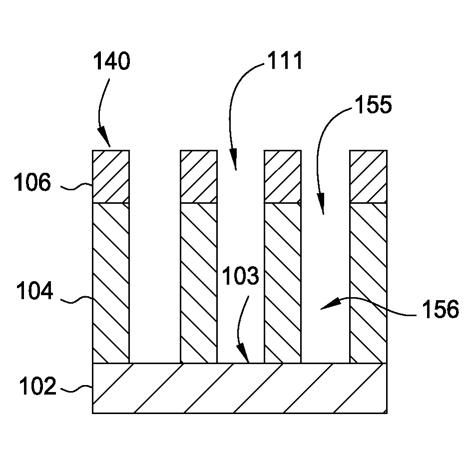
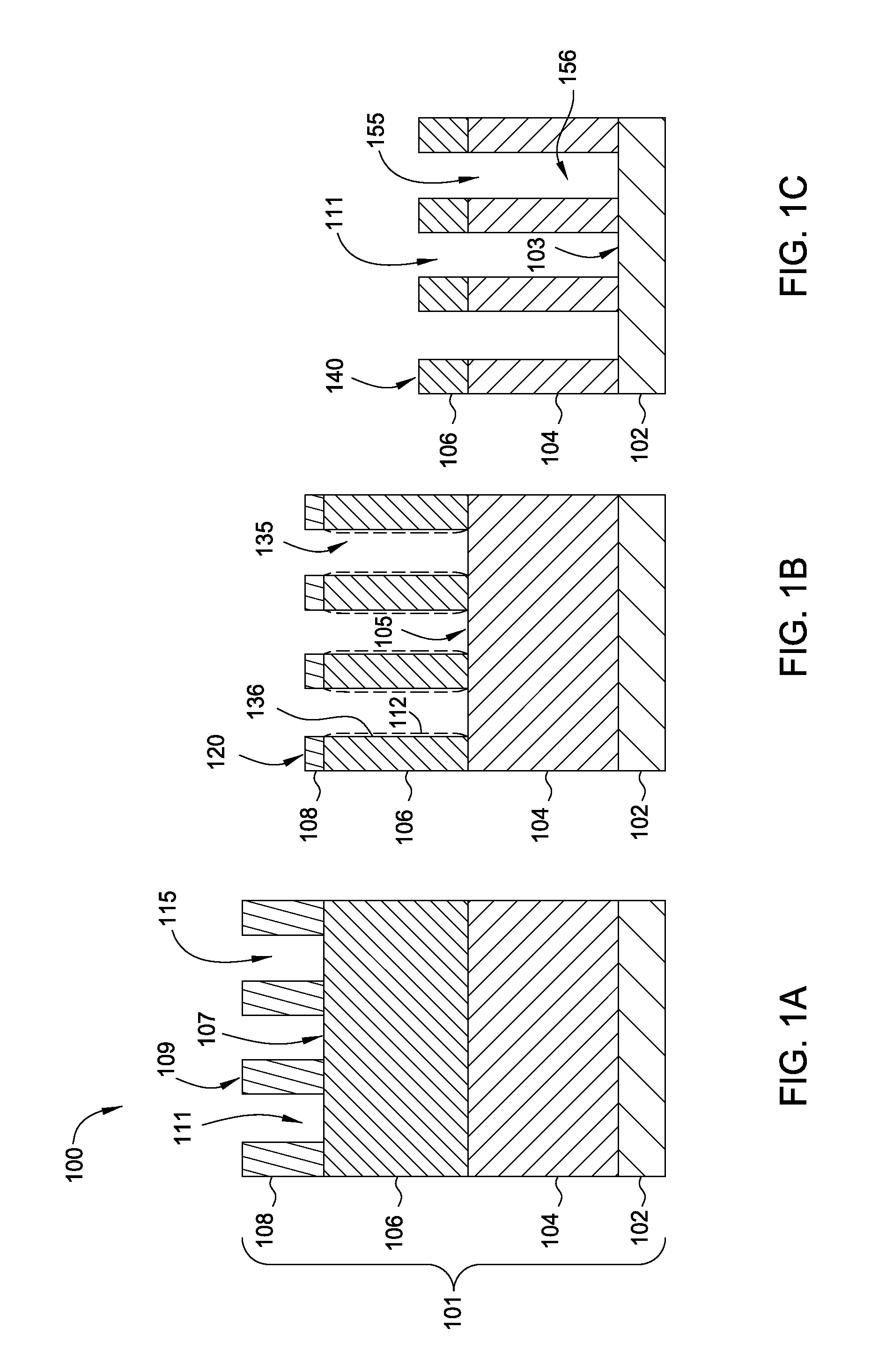
[0018]A boron doped hardmask layer, which may include between 1% by weight and 40% by weight boron (B), may be located directly on a semiconductor layer, such as a substrate, and provide a mask thereon for ion implanting or diffusing of dopants into the substrate. The boron doped hardmask layer may also be used in the formation of openings in an underlying deposited film layer. The openings may be used to form interconnects, as well as other features and devices, such as raised gates, capacitors, etc, on the substrate.

[0019]The embodiments described herein disclose methods for patterning the boron doped hardmask layer. The boron doped hardmask layer may be used to etch an underlying material for the formation of features with high aspect ratios and / or with small dimensions therein. As discussed herein, high aspect ratio of the features refers to the submicron structures having aspect ratios in excess of 4:1, and small dimensions refer to the submicron structures having dimensions ab...


PUM


Abstract

In one embodiment, a method is proposed for etching a boron dope hardmask layer. The method includes flowing a process gas comprising at least CH4 into a processing chamber. Forming a plasma in the process chamber from the process gas and etching the boron doped hardmask layer in the presence of the plasma. In other embodiments, the process gas utilized to etch the boron doped hardmask layer includes CH4, Cl2, SF6 and O2.

Description

CROSS-REFERENCE TO RELATED APPLICATIONS[0001]This application claims benefit of U.S. Provisional Application Ser. No. 61 / 872,456, filed Aug. 30, 2013 (Attorney Docket No. APPM / 20917USL), of which is incorporated by reference in its entirety.BACKGROUND OF THE DISCLOSURE[0002]1. Field of the Invention[0003]The embodiments herein generally relate to patterning a semiconductor substrate and more particularly, the chemistries used in etching a boron doped hardmask layer.[0004]2. Description of the Background Art[0005]Reliably producing submicron and smaller features is one of the key requirements of very large scale integration (VLSI) and ultra large scale integration (ULSI) of semiconductor devices. However, with the continued miniaturization of circuit technology, the dimensions of the size and pitch of circuit features, such as interconnects, have placed additional demands on processing capabilities. The multilevel interconnects that lie at the heart of this technology require precise...

Claims


Application Information

Patent Timeline
IPC IPC(8): H01L21/033
CPCH01L21/0337H01L21/0338H01L21/0332H01J37/32082H01J37/3244H01J2237/334H01L21/31122H01L21/6831
Inventor KONG, BYUNGKOOKKIM, JUN WANAHN, WONMOYOO, JEONG HYUNKIM, HUN SANG
Owner APPLIED MATERIALS INC
Why Eureka
Try Eureka