

Group iii nitride semiconductor multilayer substrate and group iii nitride semiconductor field effect transistor
a semiconductor field effect transistor and multilayer substrate technology, applied in the direction of transistors, semiconductor devices, electrical devices, etc., can solve the problems of insufficient suppression of current collapse, and achieve the effect of suppressing current collaps
- Summary
- Abstract
- Description
- Claims
- Application Information
AI Technical Summary
Benefits of technology
Problems solved by technology
Method used
Image

Examples
first embodiment
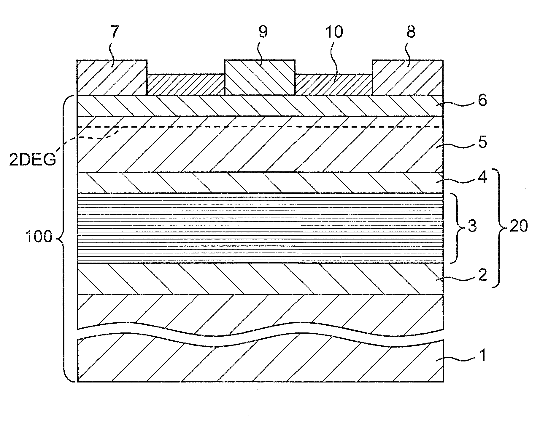
[0047]FIG. 1 is a sectional view of a nitride semiconductor device including a group III nitride semiconductor multilayer substrate 100 according to a first embodiment of the invention. This nitride semiconductor device is a GaN-related HFET (Hetero-junction Field Effect Transistor).
[0048]In the nitride semiconductor device, as shown in FIG. 1, an AlN seed layer 2, a superlattice layer 3, a carbon-doped GaN layer 4, a channel GaN layer 5 as an example of a channel layer, and an AlGaN barrier layer 6 as an example of a barrier layer are formed sequentially on a Si substrate 1. The AlN seed layer 2, the superlattice layer 3, and the carbon-doped GaN layer 4 constitute a buffer layer 20. Also, the Si substrate 1, the AlN seed layer 2, the superlattice layer 3, the carbon-doped GaN layer 4, the channel GaN layer 5 and the AlGaN barrier layer 6 constitute the group III nitride semiconductor multilayer substrate 100.
[0049]A source electrode 7 and a drain electrode 8 are formed on the AlGa...
second embodiment
[0094]FIG. 4A is a sectional view of a group III nitride semiconductor multilayer substrate 200 according to a second embodiment of the invention.
[0095]In this group III nitride semiconductor multilayer substrate 200 of the second embodiment, an AlN seed layer 202, a superlattice buffer layer 203, a pressure-proof use carbon-doped GaN layer 204, a channel GaN layer 205 as an example of a channel layer, and a barrier layer 206 are formed sequentially on a Si substrate 201.
[0096]The Si substrate 201, the AlN seed layer 202, the superlattice layer 203, the carbon-doped GaN layer 204, the channel GaN layer 205 and the barrier layer 206 constitute the group III nitride semiconductor multilayer substrate 200.
[0097]On the barrier layer 206 of the group III nitride semiconductor multilayer substrate 200, although not shown, a source electrode, a drain electrode, a gate electrode and an insulating film are formed, as in the case of the first embodiment described above. The source electrode, ...
PUM
| Property | Measurement | Unit |
|---|---|---|
| depths | aaaaa | aaaaa |
| length | aaaaa | aaaaa |
| thickness | aaaaa | aaaaa |
Abstract
Description
Claims
Application Information