X-ray Diffraction (XRD) Characterization Methods for Sigma=3 Twin Defects in Cubic Semiconductor (100) Wafers

a cubic semiconductor and twin defect technology, applied in the direction of material analysis using radiation diffraction, instruments, measurement devices, etc., can solve the problems of affecting the performance of electronic devices made from semiconductor materials, and affecting the performance of semiconductor materials. , to achieve the effect of reducing/eliminating defects in wafers, rapid modification of wafer fabrication processes, and short tim

Active Publication Date: 2015-03-19
NASA
View PDF21 Cites 7 Cited by
  • Summary
  • Abstract
  • Description
  • Claims
  • Application Information

AI Technical Summary

Benefits of technology

[0009]The method / processes of the present invention do not require contact or treatment of the materials being tested. The methods / processes can be utilized to provide a pass / fail (quality factor) measurement of individual wafers in a very short time. Thus, the methods / processes can be utilized in connection with commercial wafer fabrication processes to ensure that the wafers that are produced meet predefined quality / defect criteria. Furthermore, the results of XRD testing / methods / processes according to the present invention can be utilized to identify problems in water fabrication processes whereby the process can be modified to reduce / eliminate defects in the wafers. Significantly, the defect measurement methods / processes of the present invention can be integrated into wafer fabrication processes to provide “real time” feedback that can be utilized to rapidly modify the wafer fabrication process and reduce the number of defective wafers that are fabricated.

Problems solved by technology

Various crystal structure defects may be present in semiconductor materials.
Such defects may adversely affect the performance of electronic devices made from semiconductor materials.
However, known defect measuring techniques (e.g. TEM and Etch-pit density test) damage or destroy the wafer, and the damaged wafer is typically useless after testing.

Method used


Image

  • X-ray Diffraction (XRD) Characterization Methods for Sigma=3 Twin Defects in Cubic Semiconductor (100) Wafers
  • X-ray Diffraction (XRD) Characterization Methods for Sigma=3 Twin Defects in Cubic Semiconductor (100) Wafers
  • X-ray Diffraction (XRD) Characterization Methods for Sigma=3 Twin Defects in Cubic Semiconductor (100) Wafers

Examples


Embodiment Construction

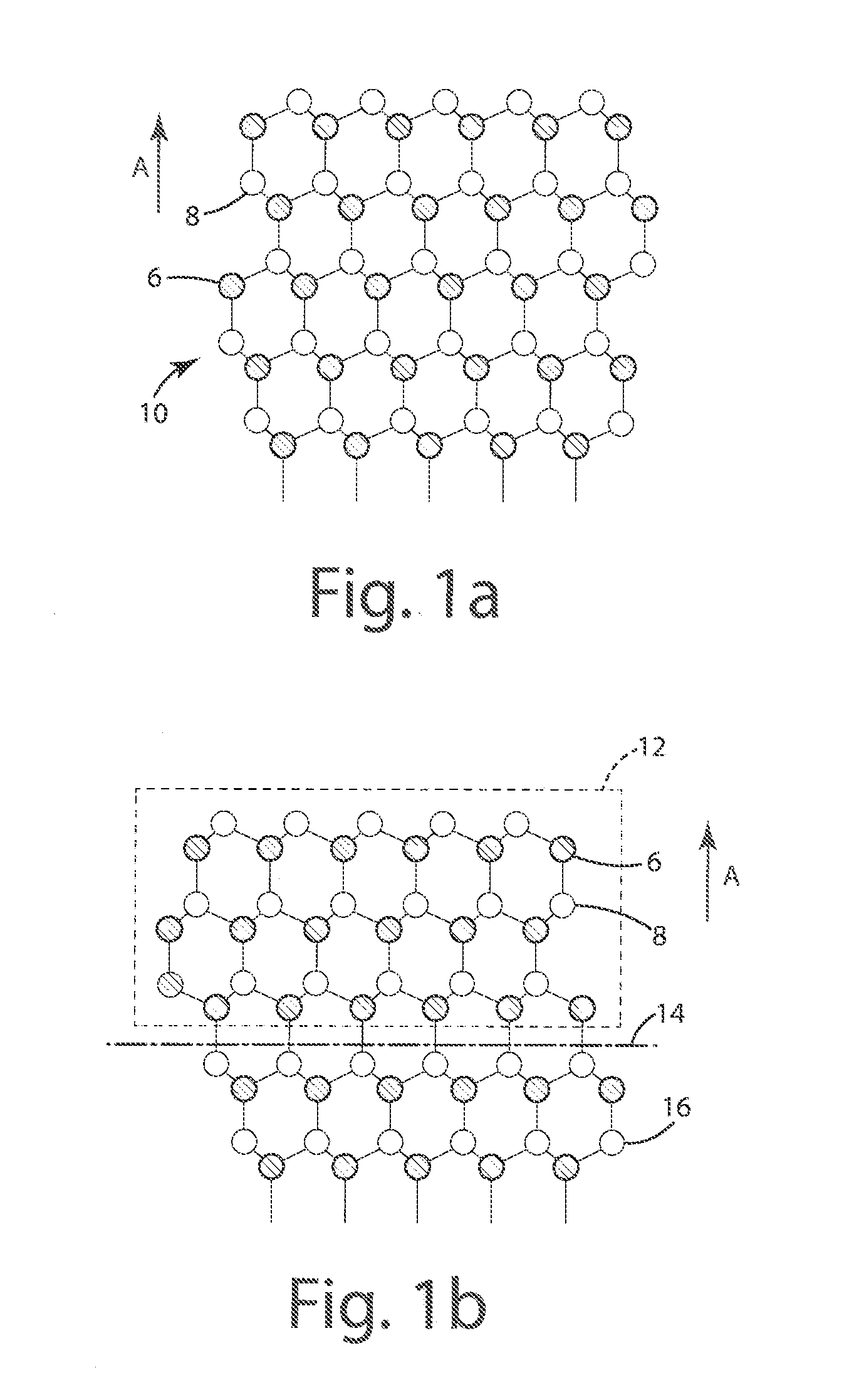
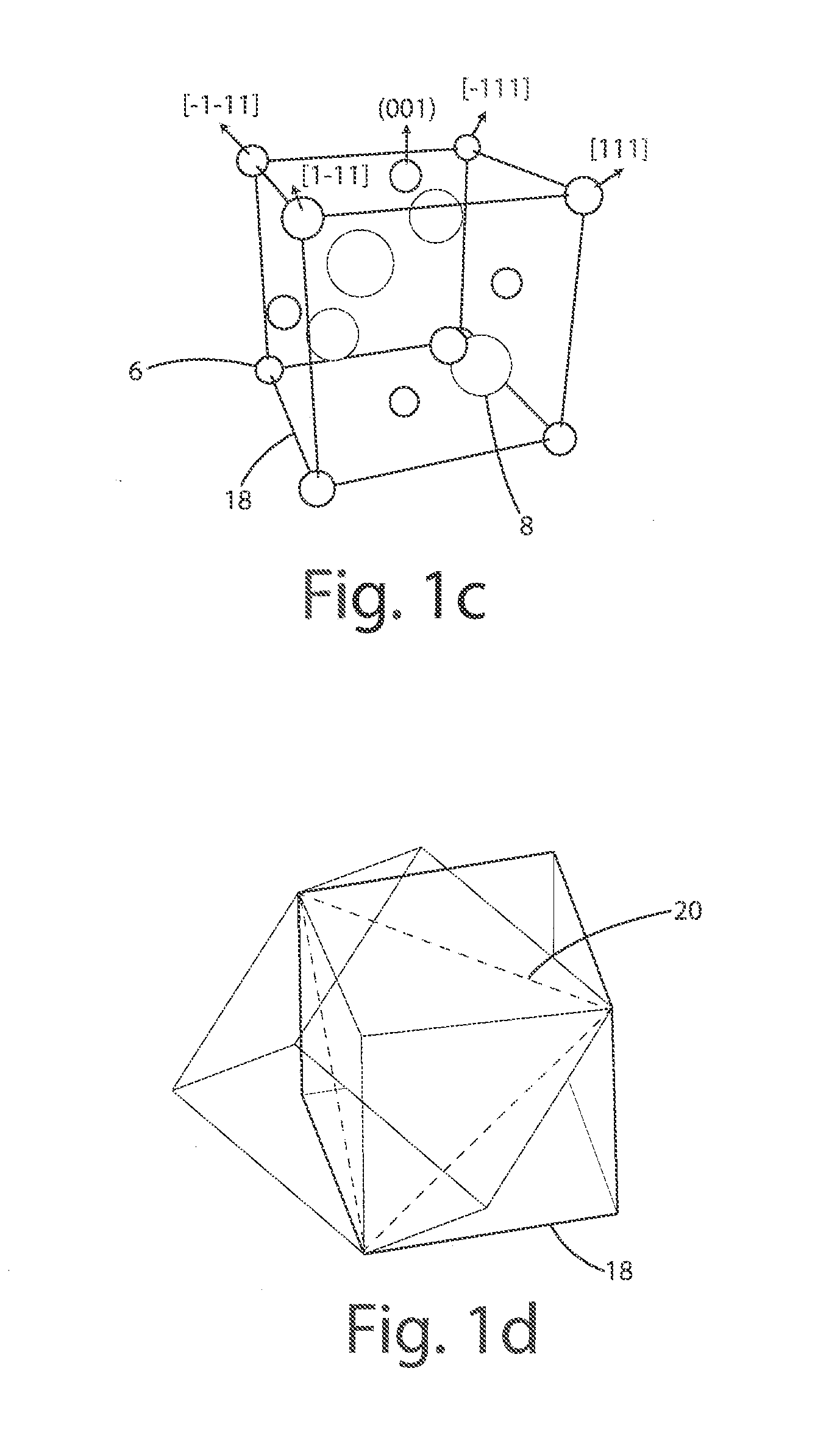
[0027]For purposes of description herein, the terms “upper,”“lower,”“right,”“let”“rear,”“front,”“vertical,”“horizontal,” and derivatives thereof shall relate to the invention as oriented in FIG. 1. However, it is to be understood that the invention may assume various alternative orientations and step sequences, except where expressly specified to the contrary. It is also to be understood that the specific devices and processes illustrated in the attached drawings, and described in the following specification, are simply exemplary embodiments of the inventive concepts defined in the appended claims. Hence, specific dimensions and other physical characteristics relating to the embodiments disclosed herein are not to be considered as limiting, unless the claims expressly state otherwise.

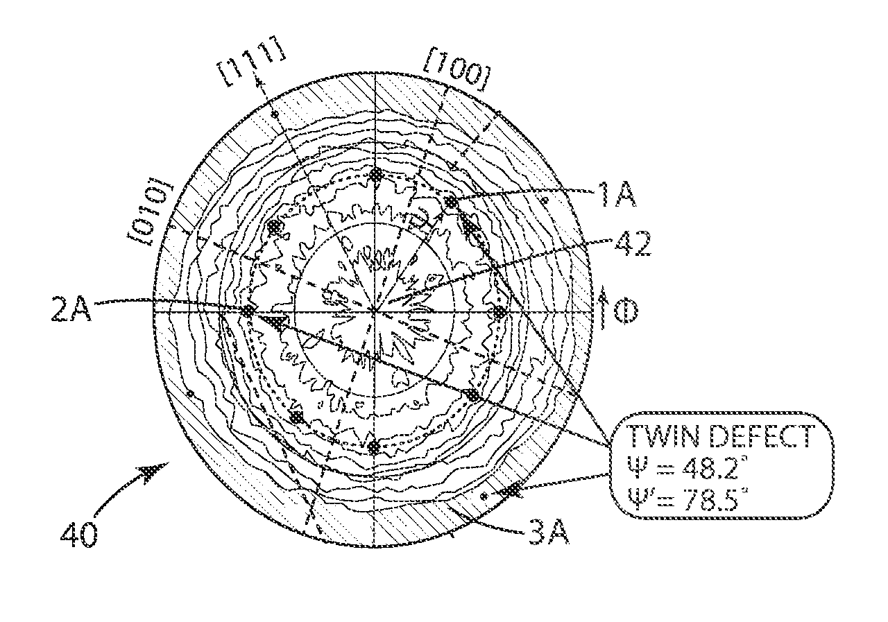
[0028]As discussed in more detail below, one aspect of the present invention is a process or method for determining a quality factor comprising a ratio as defined in equations 1.0, 1.1, and 1.2 below. T...


PUM

PropertyMeasurementUnit
tilt angleaaaaaaaaaa

Abstract

An X-ray defraction (XRD) characterization method for sigma=3 twin defects in cubic semiconductor (100) wafers includes a concentration measurement method and a wafer mapping method for any cubic tetrahedral semiconductor wafers including GaAs (100) wafers and Si (100) wafers. The methods use the cubic semiconductor's (004) pole figure in order to detect sigma=3 / {111} twin defects. The XRD methods are applicable to any (100) wafers of tetrahedral cubic semiconductors in the diamond structure (Si, Ge, C) and cubic zinc-blende structure (InP, InGaAs, CdTe, ZnSe, and so on) with various growth methods such as Liquid Encapsulated Czochralski (LEC) growth, Molecular Beam Epitaxy (MBE), Organometallic Vapor Phase Epitaxy (OMVPE), Czochralski growth and Metal Organic Chemical Vapor Deposition (MOCVD) growth.

Description

CROSS-REFERENCE TO RELATED PATENT APPLICATION(S)[0001]This patent application claims the benefit of and priority to U.S. Provisional Patent Application No. 61 / 877,416, entitled “X-RAY DIFFRACTION (XRD) CHARACTERIZATION METHODS FOR SIGMA=3 TWIN DEFECTS IN CUBIC SEMICONDUCTOR (100) WAFERS” filed on Sep. 13, 2013, the contents of which are hereby incorporated by reference in their entirety.STATEMENT REGARDING FEDERALLY SPONSORED RESEARCH OR DEVELOPMENT[0002]The invention described herein was made in the performance of work under a NASA contract and by employees of the United States Government and is subject to the provisions of Public Law 96-517 (35 U.S.C. §202) and may be manufactured and used by or for the Government for governmental purposes without the payment of any royalties thereon or therefore. In accordance with 35 U.S.C. §202, the contractor elected not to retain title.BACKGROUND OF THE INVENTION[0003]Semiconductor materials are widely utilized in numerous electronic devices....

Claims


Application Information

Patent Timeline
Patent Type & Authority Applications(United States)
IPC IPC(8): G01N23/207
CPCG01N23/207G01N23/20G01N2223/0566G01N2223/6116G01N2223/646G01N2223/6462
Inventor PARK, YEONJOONKIM, HYUN JUNGSKUZA, JONATHAN R.LEE, KUNIKKING, GLEN C.CHOI, SANG HYOUK
Owner NASA
Why Eureka
Try Eureka