Semiconductor memory devices and memory systems including the same

Active Publication Date: 2015-03-26
SAMSUNG ELECTRONICS CO LTD
View PDF8 Cites 17 Cited by
  • Summary
  • Abstract
  • Description
  • Claims
  • Application Information

AI Technical Summary

Benefits of technology

The patent text describes a semiconductor memory device that can provide a consecutive address space without including redundant cells. The device includes a memory cell array and an error correction code (ECC) circuit. The memory cell array is divided into two memory regions, each containing multiple pages of memory cells. The ECC circuit corrects single-bit errors in the first memory region using parity bits. The first memory region provides a consecutive address space to an external memory controller, while the second memory region is reserved for repairing failed pages. The device can also include a page control circuit that selects any page in the first or second memory region for replacement with a page of the other region. Overall, the semiconductor memory device provides a consecutive address space without the need for redundant cells.

Problems solved by technology

Due to limits of semiconductor micro-manufacturing processes, there is a general tradeoff between memory density and reliability.
For example, as memory density increases, reliability tends to decrease typically.
This reduction in reliability often leads to bad cells, which can reduce semiconductor yield.
In example embodiments, the first failed page may have a multi-bit error.

Method used


Image

  • Semiconductor memory devices and memory systems including the same
  • Semiconductor memory devices and memory systems including the same
  • Semiconductor memory devices and memory systems including the same

Examples


Embodiment Construction

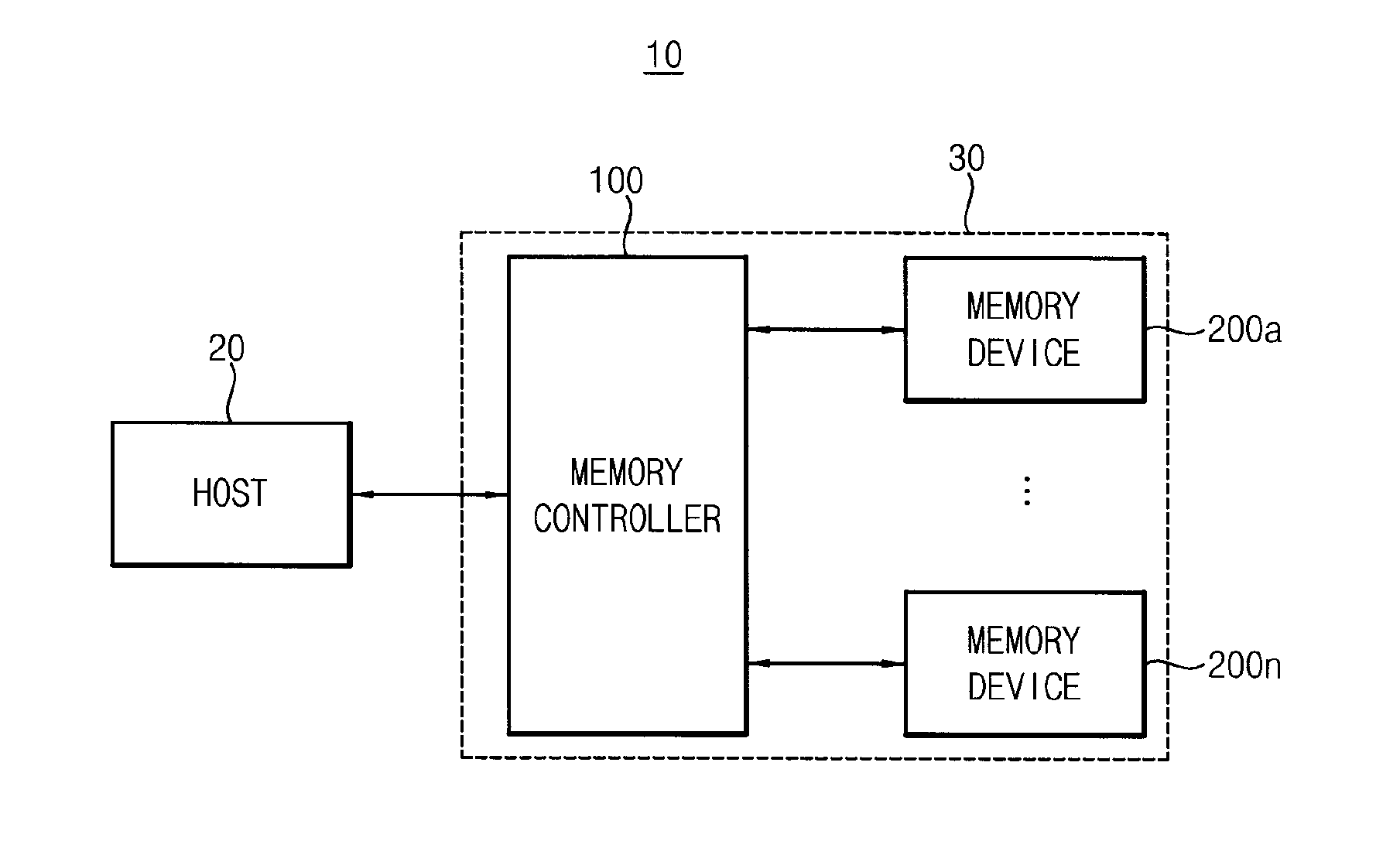
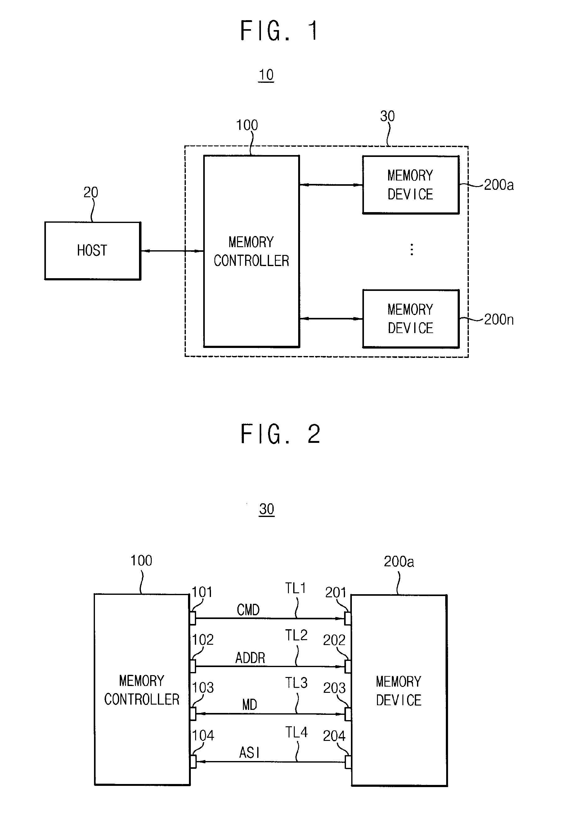
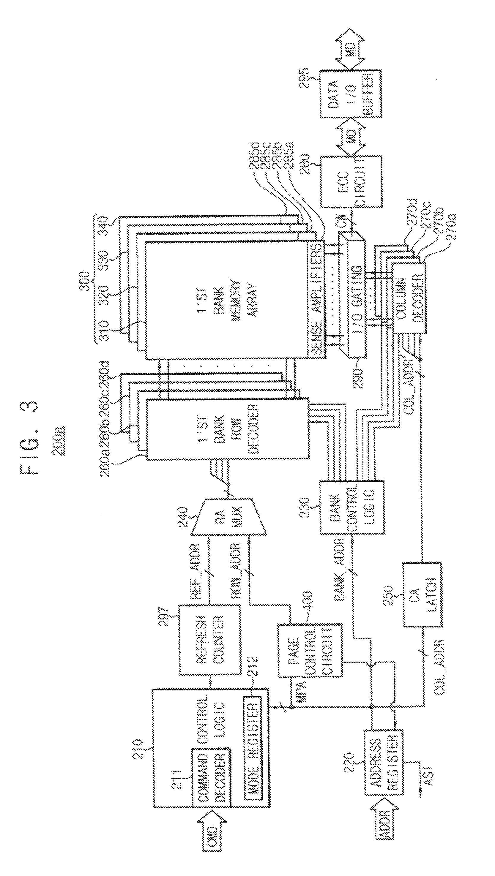
[0049]Various exemplary embodiments will be described more fully hereinafter with reference to the accompanying drawings, in which some exemplary embodiments are shown. The present disclosure may, however, be embodied in many different forms and should not be construed as limited to the example embodiments set forth herein. These example embodiments are just that examples and many implementations and variations are possible that do not require the details provided herein. In the drawings, the sizes and relative sizes of layers and regions may be exaggerated for clarity. Like numerals refer to like elements throughout.

[0050]It will be understood that, although the terms first, second, third etc. may be used herein to describe various elements, these elements should not be limited by these terms. Unless indicated otherwise, these terms are used to distinguish one element from another. Thus, a first element discussed below could be termed a second element without departing from the tea...


PUM


Abstract

The semiconductor memory device includes a memory cell array and an error correction code (ECC) circuit. The memory cell array is divided into a first memory region and a second memory region. Each of the first and second memory regions includes a plurality of pages each page including a plurality of memory cells connected to a word line. The ECC circuit corrects single-bit errors of the first memory region using parity bits. The first memory region provides a consecutive address space to an external device by correcting the single-bit errors using the ECC circuit and the second memory region is reserved for repairing at least one of a first failed page of the first memory region or a second failed page of the second memory region.

Description

CROSS-REFERENCE TO RELATED APPLICATION(S)[0001]This US non-provisional application claims the benefit of priority under 35 USC §119 to Korean Patent Application No. 10-2013-0113641, filed on Sep. 25, 2013, in the Korean Intellectual Property Office (KIPO), the contents of which are incorporated herein in their entirety by reference.BACKGROUND[0002]1. Technical Field[0003]Exemplary embodiments relate to semiconductor memory devices, and more particularly to a semiconductor memory device and a memory system including the same.[0004]2. Discussion of the Related Art[0005]Memory devices are employed in various electronic systems. Electronic systems typically require high-density memory devices. Due to limits of semiconductor micro-manufacturing processes, there is a general tradeoff between memory density and reliability. For example, as memory density increases, reliability tends to decrease typically. This reduction in reliability often leads to bad cells, which can reduce semiconducto...

Claims


Application Information

Patent Timeline
IPC IPC(8): G06F11/16
CPCG06F11/167G06F11/1048G06F11/10G06F12/00G11C29/76G11C29/886
Inventor YOUN, JAE-YOUNPARK, CHUL-WOOYU, HAK-SOO
Owner SAMSUNG ELECTRONICS CO LTD
Why Eureka
Try Eureka