Semiconductor device
- Summary
- Abstract
- Description
- Claims
- Application Information
AI Technical Summary
Benefits of technology
Problems solved by technology
Method used
Image

Examples
embodiment 1
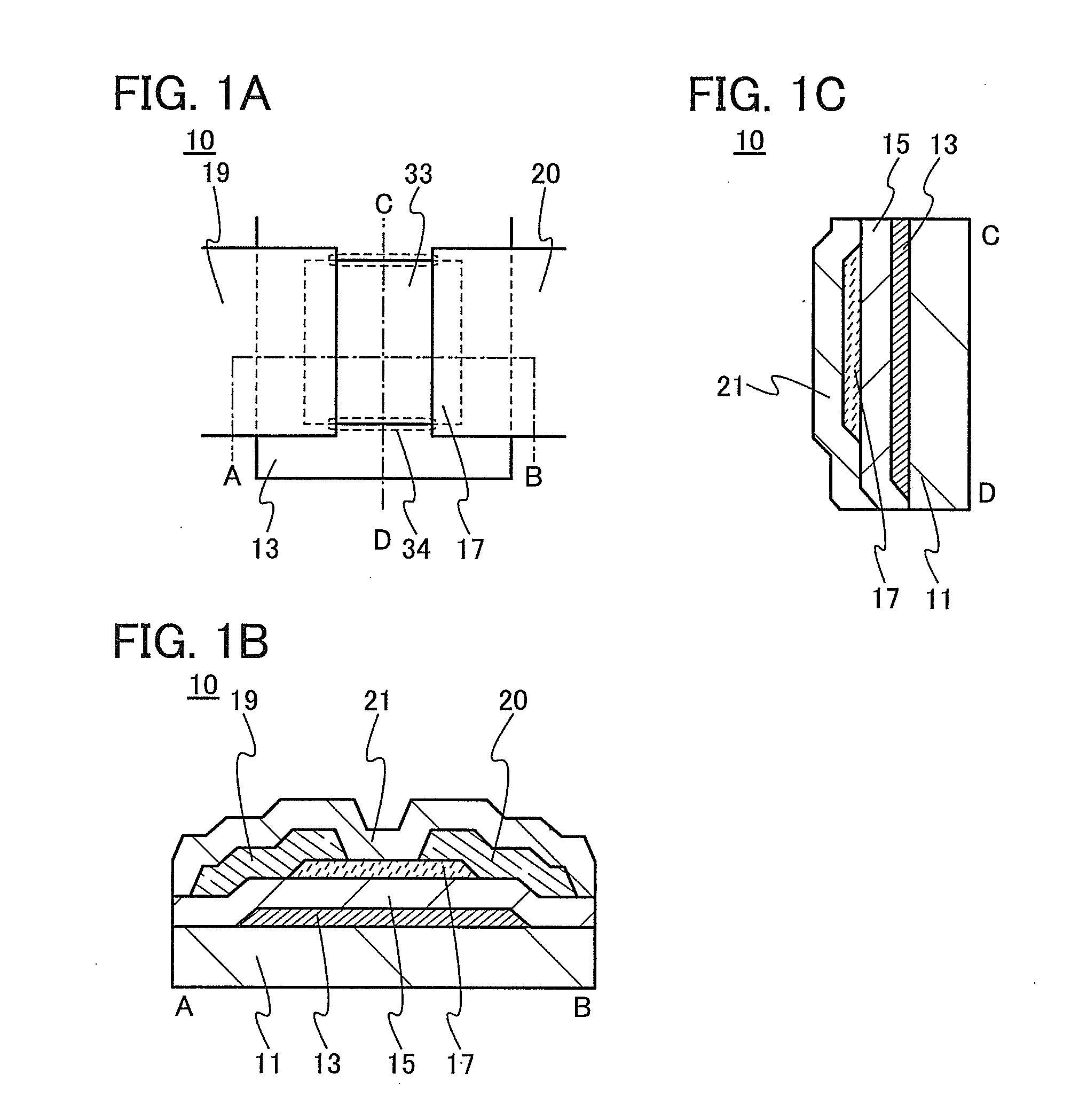
[0111]In this embodiment, a semiconductor device of one embodiment of the present invention and a method for manufacturing the semiconductor device are described with reference to drawings. A transistor 10 described in this embodiment has a bottom-gate structure.
[0112]FIGS. 1A to 1C are a top view and cross-sectional views of the transistor 10 included in a semiconductor device. FIG. 1A is a top view of the transistor 10. FIG. 1B is a cross-sectional view taken along dashed-dotted line A-B in FIG. 1A, and FIG. 1C is a cross-sectional view taken along dashed-dotted line C-D in FIG. 1A. Note that in FIG. 1A, a substrate 11, a gate insulating film 15. a protective film 21, and the like are omitted for simplicity.
[0113]The transistor 10 illustrated in FIGS. 1A to 1C includes a gate electrode 13 over the substrate 11, the gate insulating film 15 over the substrate 11 and the gate electrode 13. an oxide semiconductor film 17 overlapping with the gate electrode 13 with the gate insulating ...
modification example 3
[0248]Modification examples of the transistor 10 described in this embodiment are described with reference to FIGS. 6A to 6C. The transistor 10 described in this embodiment includes one gate electrode; in contrast, a transistor 10e described in this modification example includes two gate electrodes with an oxide semiconductor film interposed between the gate electrodes.
[0249]A top view and cross-sectional views of the transistor 10e included in a semiconductor device are illustrated in FIGS. 6A to 6C. FIG. 6A is a top view of the transistor 10e, FIG. 6B is a cross-sectional view taken along dashed-dotted line A-B in FIG. 6A, and FIG. 6C is a cross-sectional view taken along dashed-dotted line C-D in FIG. 6A. Note that in FIG. 6A. the substrate 11, the gate insulating film 15, the protective film 21, and the like are omitted for simplicity.
[0250]The transistor 10e illustrated in FIGS. 6B and 6C is a channel-etched transistor including the gate electrode 13 over the substrate 11; the ...
modification example 4
[0253]Modification examples of the transistor 10 described in this embodiment are described with reference to FIGS. 7A to 7F and FIGS. 8A to 8C. The transistor 10 described in this embodiment includes the single-layer oxide semiconductor film; in contrast, transistors 10f and 10g described in this modification example each includes a multi-layer film.
[0254]FIGS. 7A to 7C are a top view and cross-sectional views of the transistor 10f included in a semiconductor device. FIG. 7A is a top view of the transistor 10f, FIG. 7B is a cross-sectional view taken along dashed-dotted line A-B in FIG. 7A. and FIG. 7C is a cross-sectional view taken along dashed-dotted line C-D in FIG. 7A. Note that in FIG. 7A, the substrate 11, the gate insulating film 15, the protective film 21, and the like are omitted for simplicity.
[0255]The transistor 10f illustrated in FIG. 7A includes a multilayer film 45 overlapping with the gate electrode 13 with the gate insulating film 15 provided therebetween, and the...
PUM
 Abstract
Description
Claims
Application Information
 - Generate Ideas
- Intellectual Property
- Life Sciences
- Materials
- Tech Scout
- Unparalleled Data Quality
- Higher Quality Content
- 60% Fewer Hallucinations
Browse by: Latest US Patents, China's latest patents, Technical Efficacy Thesaurus, Application Domain, Technology Topic, Popular Technical Reports.
© 2025 PatSnap. All rights reserved.Legal|Privacy policy|Modern Slavery Act Transparency Statement|Sitemap|About US| Contact US: help@patsnap.com