Light emitting device and atomic oscillator

a technology which is applied in the field of light emitting devices and atomic oscillators, can solve the problems of difficult to vary the wavelength with a small variation, large wavelength variation, and light emitting devices, and achieve the effect of suppressing the refractive index variation and surely polarizing the light generated

Active Publication Date: 2015-04-16
SEIKO EPSON CORP
View PDF1 Cites 2 Cited by
  • Summary
  • Abstract
  • Description
  • Claims
  • Application Information

AI Technical Summary

Benefits of technology

[0029]According to such an atomic oscillator as described above, it is possible to inhibit the refractive index variation due to the photoelastic effect and the refractive index variation due to the electrooptic effect in the third semiconductor multilayer film mirror from being canceled out with each other in the effective refractive index in the stacking direction of the first semiconductor multilayer film mirror and the active layer. As a result, it is possible to more surely polarize the light generated in the active layer.

Problems solved by technology

However, in the light emitting device of JP-A-10-270799, since the wavelength of the light to be emitted is varied due to the absorption of the light in the wavelength conversion section, the variation in the wavelength is large, and it is difficult to vary the wavelength with a small variation.
Therefore, the light emitting device of JP-A-10-270799 cannot control the wavelength with high accuracy, and cannot be used as a light source of the atomic oscillator.
In the case of, for example, injecting the current into the active layer to control the center frequency, since the light output also varies in accordance with the injection amount of the current, the control becomes complicated.

Method used


Image

  • Light emitting device and atomic oscillator
  • Light emitting device and atomic oscillator
  • Light emitting device and atomic oscillator

Examples


first embodiment

1. First Embodiment

1.1. Light Emitting Device

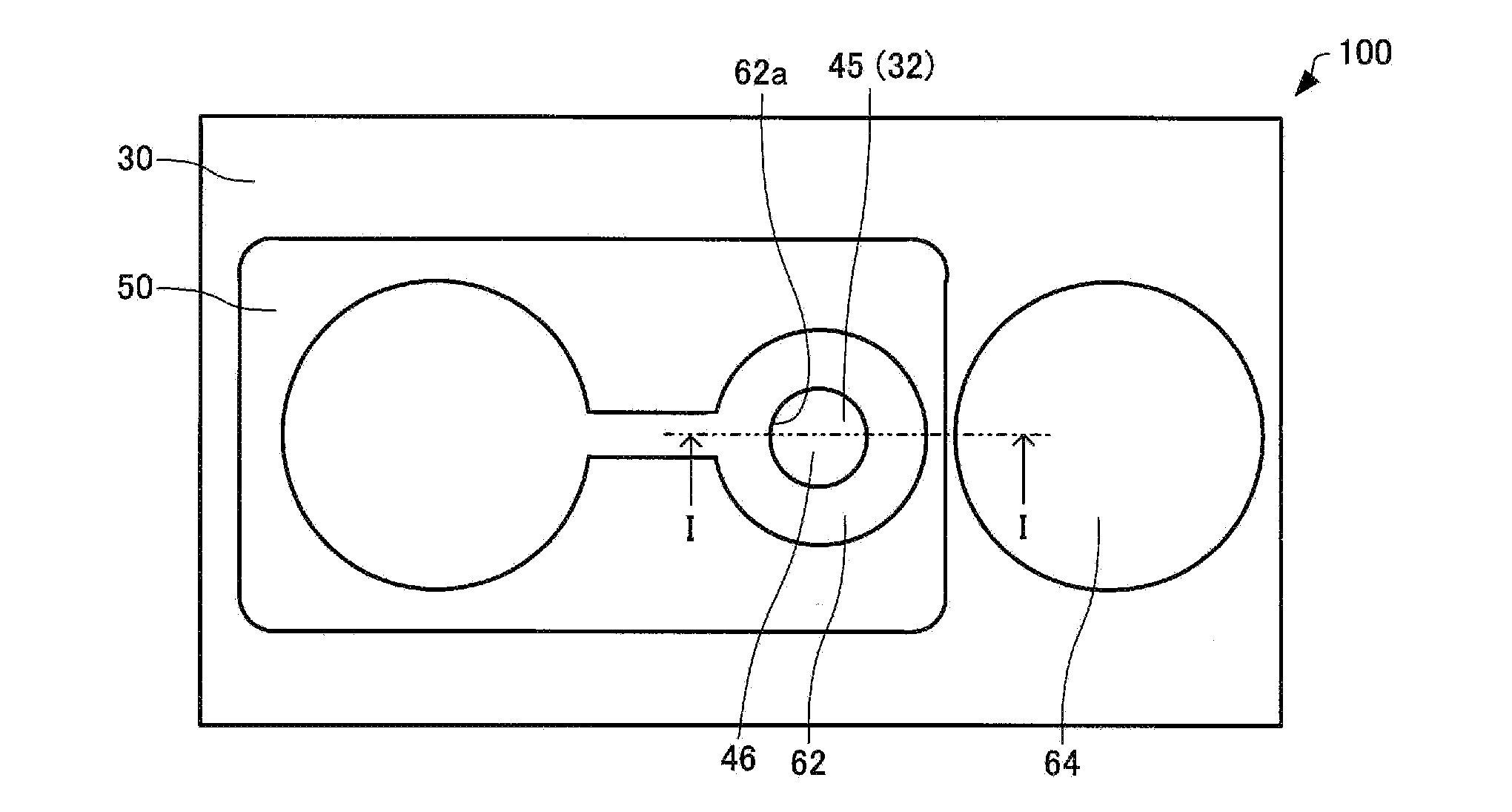
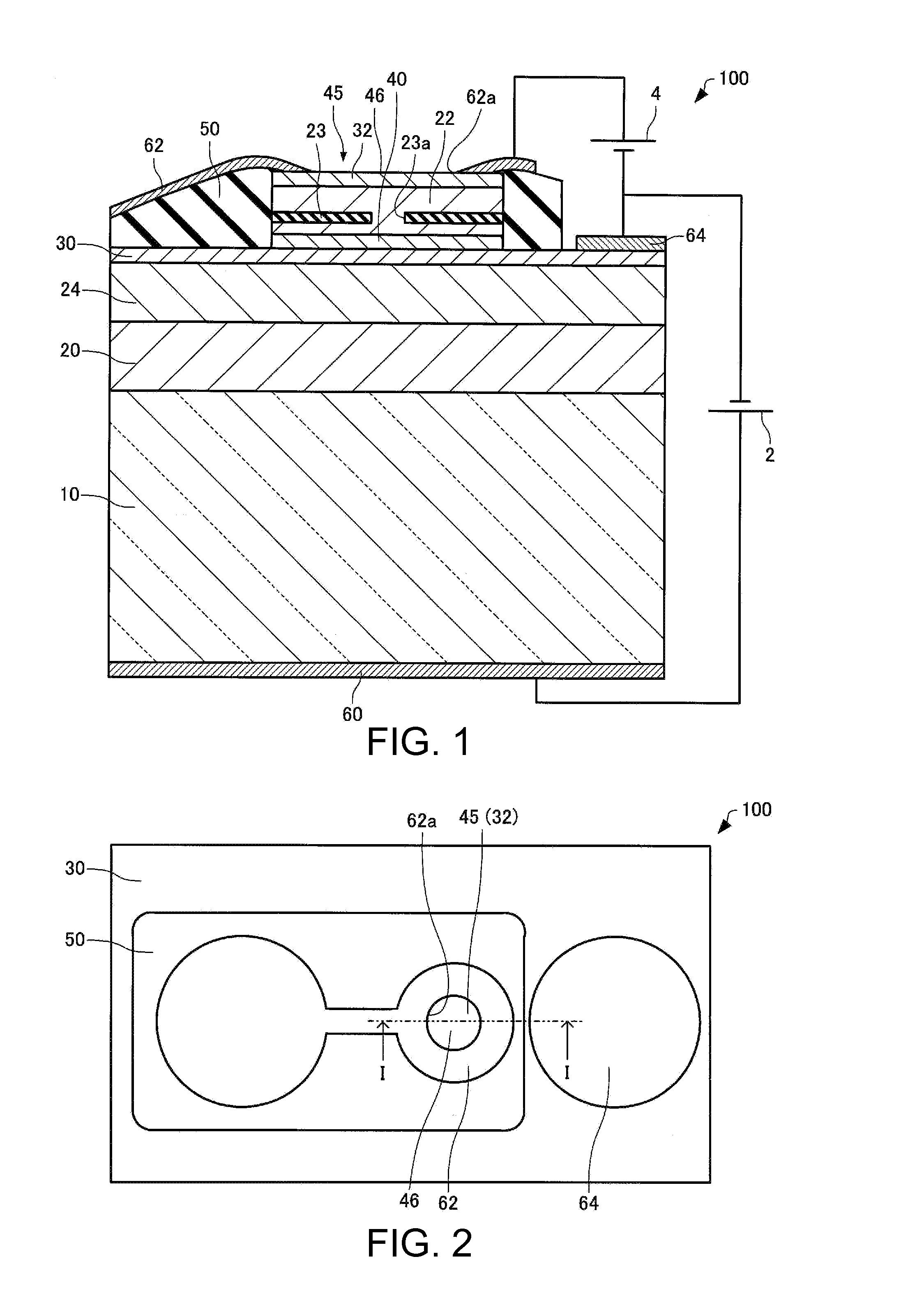
[0049]Firstly, a light emitting device according to a first embodiment will be explained with reference to the accompanying drawings. FIG. 1 is a cross-sectional view schematically showing the light emitting device 100 according to the first embodiment. FIG. 2 is a plan view schematically showing the light emitting device 100 according to the first embodiment. It should be noted that FIG. 1 is a cross-sectional view along the I-I line shown in FIG. 2.

[0050]As shown in FIGS. 1 and 2, the light emitting device 100 includes a substrate 10, a first semiconductor multilayer mirror 20, a second semiconductor multilayer film mirror 22, a third semiconductor multilayer film mirror 24, a first contact layer 30, a second contact layer 32, an active layer 40, an insulating layer 50, a first electrode 60, a second electrode 62, and a third electrode 64. The light emitting device 100 is a surface emitting semiconductor laser (Vertical Cavity Surface E...

experimental example

1.3. Experimental Example

[0090]Hereinafter, an experimental example will be shown, and the present embodiment of the invention will more specifically be explained. It should be noted that the invention is not at all limited by the following experimental example.

1.3.1. Configuration of Light Emitting Device

example 1

(1) Example 1

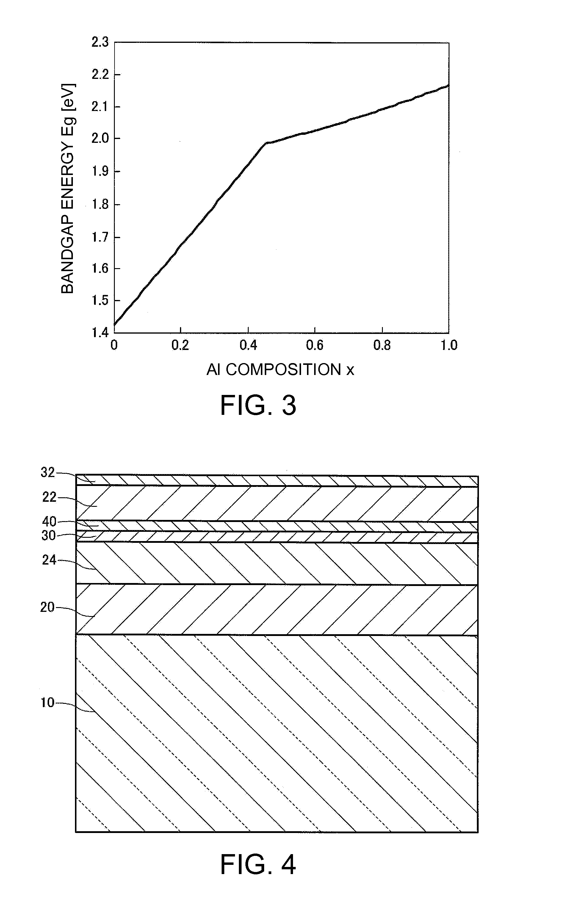
[0091]As Example 1, the light emitting device shown in FIG. 1 was used. As the substrate 10, an n-type GaAs substrate was used. As the first semiconductor multilayer film mirror 20, there was used what was obtained by alternately stacking 20 pairs of n-type Al0.15Ga0.85As layers and n-type Al0.9Ga0.1As layers on each other. As the third semiconductor multilayer film mirror 24, there was used what was obtained by alternately stacking 5 pairs of i-type Al0.15Ga0.85As layers and i-type Al0.9Ga0.1As layers on each other. As the first contact layer 30, an n-type GaAs layer was used. As the active layer 40, there was used what was obtained by stacking an n-type Al0.3Ga0.7As layer, the quantum well layer formed of an i-type GaAs layer and an i-type Al0.3Ga0.7As layer, and a p-type Al0.3Ga0.7As layer on each other. As the second semiconductor multilayer film mirror 22, there was used what was obtained by alternately stacking 25 pairs of p-type Al0.15Ga0.85As layers and p-type A...


PUM


Abstract

A light emitting device includes a first semiconductor multilayer film mirror of a first conductivity type, a second semiconductor multilayer film mirror of a second conductivity type that is different from the first conductivity type, an active layer formed between the first semiconductor multilayer film mirror and the second semiconductor multilayer film mirror, a third semiconductor multilayer film mirror of a semi-insulating type formed between the first semiconductor multilayer film mirror and the active layer, and a contact layer of the first conductivity type formed between the third semiconductor multilayer film mirror and the active layer, and the third semiconductor multilayer film mirror is formed of a material having a bandgap energy higher than an energy of light generated in the active layer.

Description

BACKGROUND[0001]1. Technical Field[0002]The present invention relates to a light emitting device and an atomic oscillator.[0003]2. Related Art[0004]In recent years, an atomic oscillator using coherent population trapping (CPT) as a quantum interference effect has been proposed, and downsizing and reduction in power consumption of the device have been expected. The atomic oscillator using CPT uses an electromagnetically induced transparency phenomenon (EIT phenomenon) that absorption of coherent light beams respectively having two wavelengths (frequencies) that are different from each other stops if an alkali metal atom is irradiated with the resonance light beams.[0005]The atomic oscillator can realize high accuracy by accurately controlling the difference (the frequency difference) between the two wavelengths described above. Therefore, it is preferable for a light emitting device (a light source) for emitting light beams respectively having the two wavelengths to have a variable w...

Claims


Application Information

Patent Timeline
Patent Type & Authority Applications(United States)
IPC IPC(8): H03L7/26H01S5/183
CPCH03L7/26H01S5/18361G04F5/145H01S5/0614H01S5/18302H01S5/18341H01S5/18313H01S5/18355H01S5/18386H01S5/18394H01S5/34313H01S2301/176H01S5/3201H01S2301/14
Inventor NISHIDA, TETSUO
Owner SEIKO EPSON CORP
Why Eureka
Try Eureka