Touch panel and method of manufacturing the same

a technology of touch panel and manufacturing method, which is applied in the field of touch panel, can solve the problems of multiple manufacturing steps, inconvenient cost-effectiveness, and difficulty in forming the subsequent elements on the sidewall of the black light-shielding layer, so as to reduce the complexity of manufacturing, increase yield and throughput, and reduce the cost

Active Publication Date: 2015-04-30
TPK GLASS SOLUTIONS XIAMEN
View PDF4 Cites 14 Cited by
  • Summary
  • Abstract
  • Description
  • Claims
  • Application Information

AI Technical Summary

Benefits of technology

[0007]According to the aforementioned, the present disclosure utilize a cutting step, a laminating step and a baking step to replace the conventional segmental printing which needs multiple manufacturing steps. The present disclosure can reduce the complexity of manufacture and lower the cost. In the meantime, the present disclosure can increase the yield and the throughput due to the reduction of the manufacturing steps needed. The baking step can further reduce the slope of the joint surface of the sensing layer, light-shielding layer and the color layer such that the sensing layer has a more robust structure and would not be broken easily at the sidewall.

Problems solved by technology

However, when the thickness of the black light-shielding layer is thick (such as 10 μm), it is hard to form the subsequent elements on the sidewall of the black light-shielding layer.
For example, when forming the subsequent sensing electrode, it is difficult to form the sensing electrode on the thick sidewall of the black light-shielding layer at the interface of the visible region and the non-visible region, which results in a broken-wire issue.
However, the segmental printing needs multiple manufacturing steps and is not cost-effective.
Besides, the multiple manufacturing steps will lower the yield and the throughput.

Method used


Image

  • Touch panel and method of manufacturing the same
  • Touch panel and method of manufacturing the same
  • Touch panel and method of manufacturing the same

Examples


Embodiment Construction

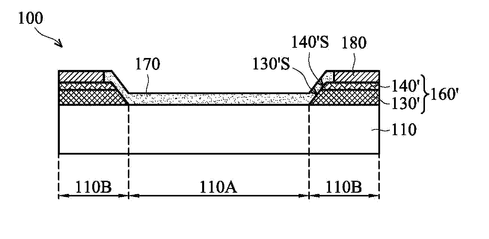
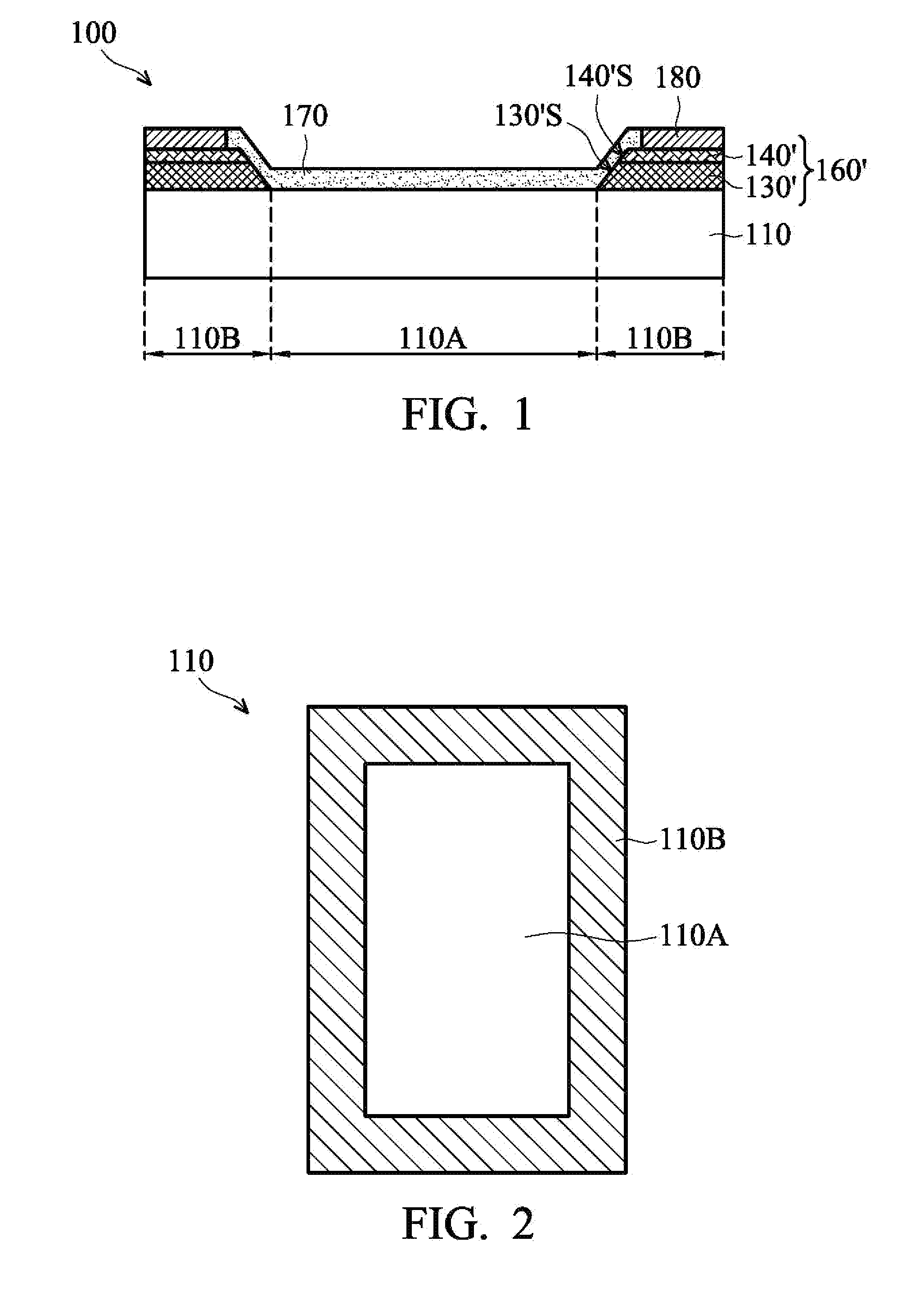
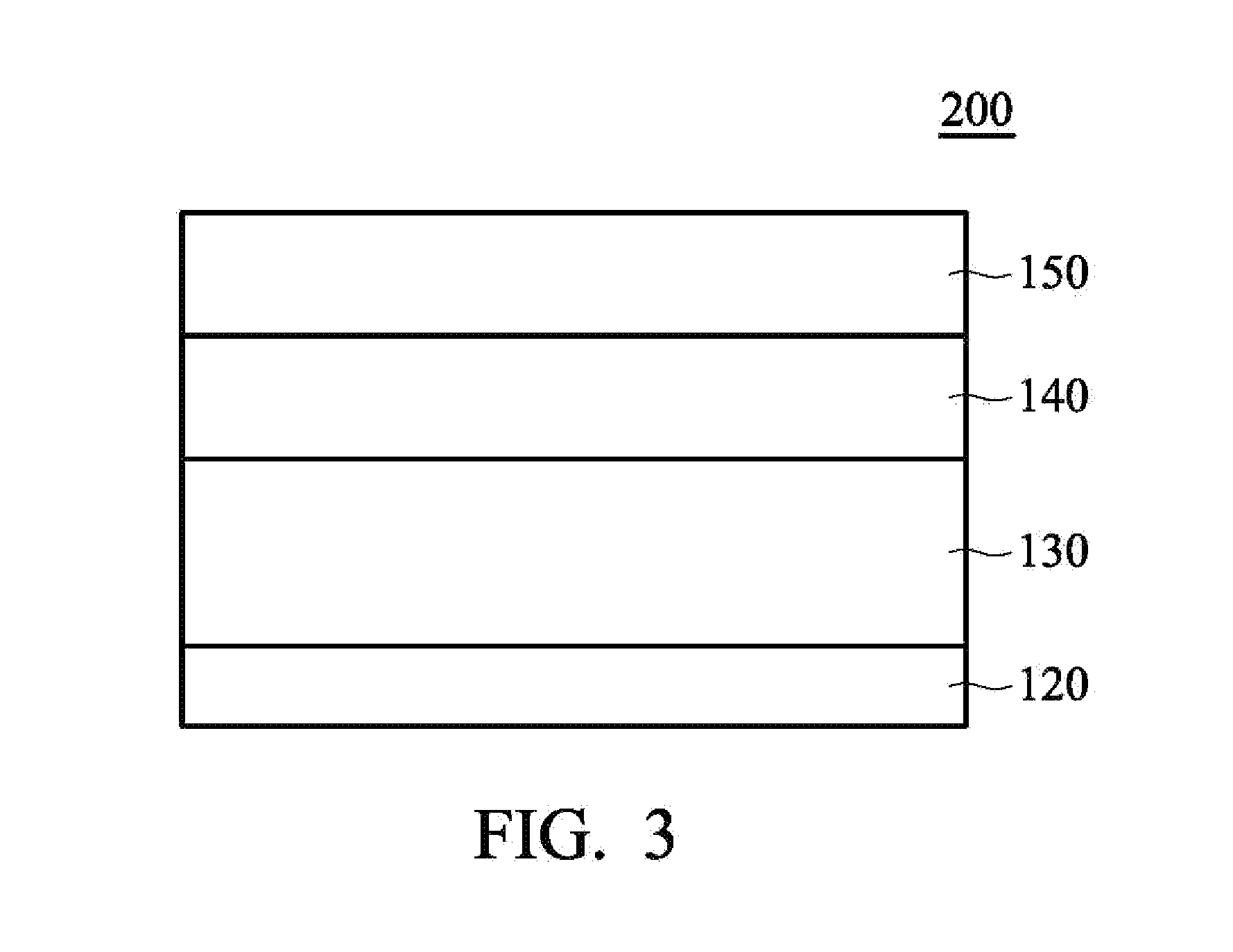
[0024]In the following detailed description, for purposes of explanation, numerous specific details are set forth in order to provide a thorough understanding of the disclosed embodiments. It will be apparent, however, that one or more embodiments can be practiced without these specific details. In other instances, well-known structures and devices are schematically shown in order to simplify the drawing.

[0025]In this specification, expressions such as “overlying the substrate”, “above the layer”, or “on the film” simply denote a relative positional relationship with respect to the surface of a base layer, regardless of the existence of intermediate layers. Accordingly, these expressions can indicate not only the direct contact of layers, but also, a non-contact state of one or more laminated layers. It is noted that in the accompanying drawings, like and / or corresponding elements are denoted to by like reference numerals.

[0026]The terms “about” and “substantially” typically means +...


PUM

PropertyMeasurementUnit
thicknessaaaaaaaaaa
thicknessaaaaaaaaaa
thicknessaaaaaaaaaa

Abstract

The present disclosure provides a touch panel, including: a substrate having a visible region and a non-visible region adjacent to at least one side of the visible region; a composite layer disposed over the non-visible region, wherein the composite layer includes a color layer and a light-shielding layer, and the color layer is disposed between the substrate and the light-shielding layer, wherein a side of the color layer adjacent to the visible region has a first inclined surface, and a side of the light-shielding layer adjacent to the visible region has a second inclined surface, wherein the first inclined surface and the second inclined surface are form a continuous surface; a sensing layer disposed over the visible region and extending to a portion of the non-visible region, wherein the sensing layer directly contacts the visible region of the substrate; and a signal wire disposed over the composite layer.

Description

BACKGROUND OF THE INVENTION[0001]This application claims priority of China Patent Application No. 201310521045.9, filed on Oct. 26, 2013, the entirety of which is incorporated by reference herein.TECHNICAL FIELD[0002]The disclosure relates to a touch panel and a method of manufacturing the same, and in particular to a method of manufacturing a touch panel by cutting, laminating and baking processes and a touch panel manufactured thereby.DESCRIPTION OF THE RELATED ART[0003]In recent years, touchscreens have gradually become the main input manner, and they have found wide application in various electronic products such as cell phones, personal digital assistants (PDA), or pocket personal computers. These touch devices usually utilize touch panels having a substrate and elements formed on the substrate, such as sensing electrodes, black light-shielding layers and touch signal wiring. The substrate can protect and support the internal elements, and the substrate can be divided into a vi...

Claims


Application Information

Patent Timeline
Patent Type & Authority Applications(United States)
IPC IPC(8): G06F3/041
CPCG06F2203/04103G06F3/041Y10T29/49124G06F3/047G06F2203/04107
Inventor TSENG, CHAN-HAOSU, SHENG-PINHUANG, CHENG-HAOCHEN, YUNG-PEIYANG, ZHIRONG
Owner TPK GLASS SOLUTIONS XIAMEN
Why Eureka
Try Eureka