Organic el device and method for manufacturing same

a technology of organic el and el luminescence, which is applied in the direction of thermoelectric device junction materials, semiconductor devices, electrical apparatus, etc., can solve the problems of adversely affecting the durability and quality of organic el devices, and achieve the effect of efficiently equalizing and reducing the distribution of ligh

Active Publication Date: 2015-05-07
KANEKA CORP
View PDF11 Cites 12 Cited by
  • Summary
  • Abstract
  • Description
  • Claims
  • Application Information

AI Technical Summary

Benefits of technology

[0065]In the configurations of the aspects of the present invention, the luminance distribution can be decreased in the emission area because the heat generated in the organic EL element during the use is efficiently equalized, and the generation of a luminous defect can be constrained because the moisture is effectively prevented from invading in the organic EL element.

Problems solved by technology

However, in the case where the organic EL element has the insufficient sealing function, a non-luminous point called a dark spot is generated after a long period of use of the organic EL device.
The growth and expansion of the dark spot adversely affect durability and quality of the organic EL device.

Method used


Image

  • Organic el device and method for manufacturing same
  • Organic el device and method for manufacturing same
  • Organic el device and method for manufacturing same

Examples


examples

[0226]A procedure to prepare the organic EL devices of the specific examples of the present invention and comparative examples and evaluation results of the specific examples and comparative examples will be described below.

first example

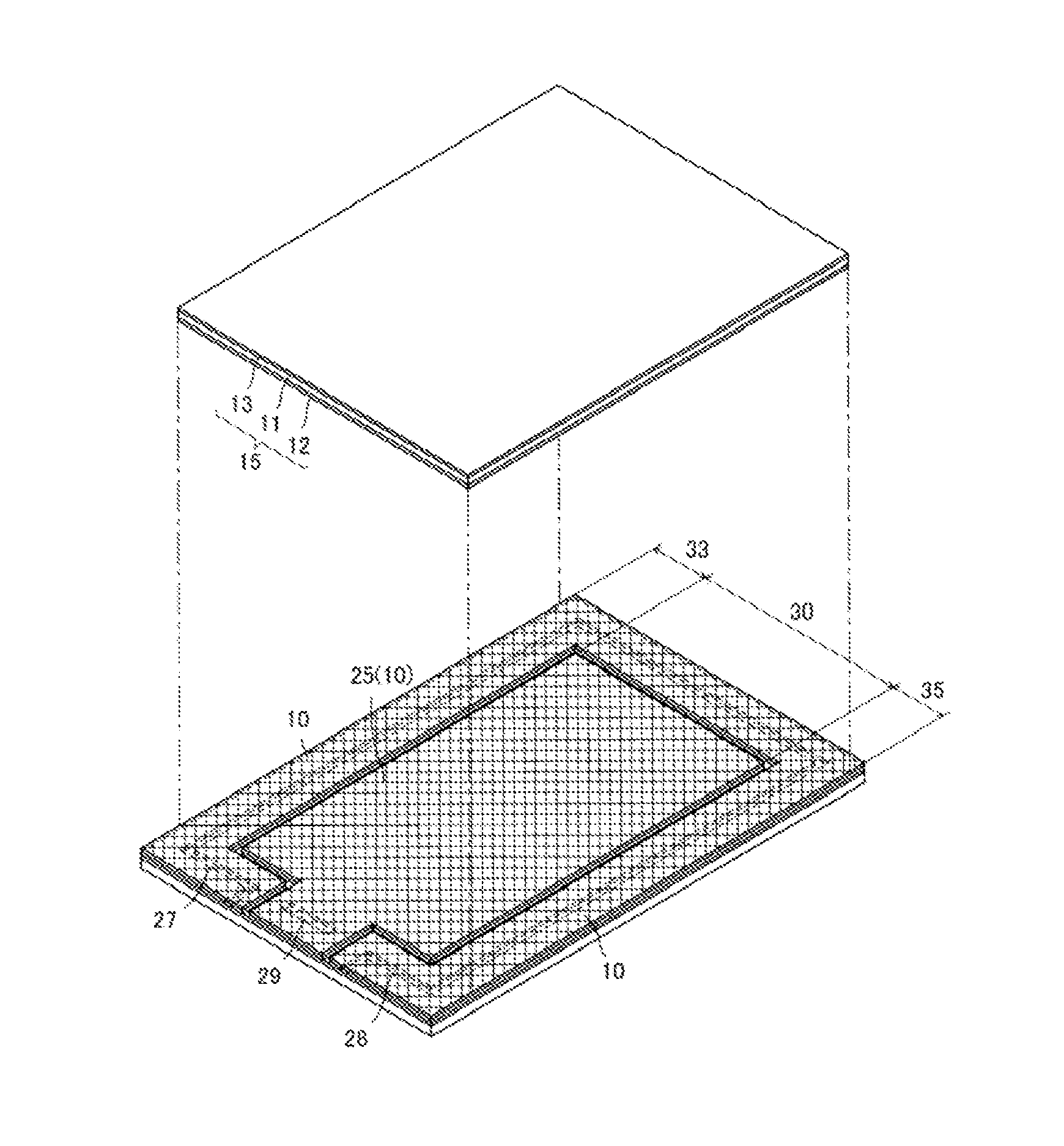
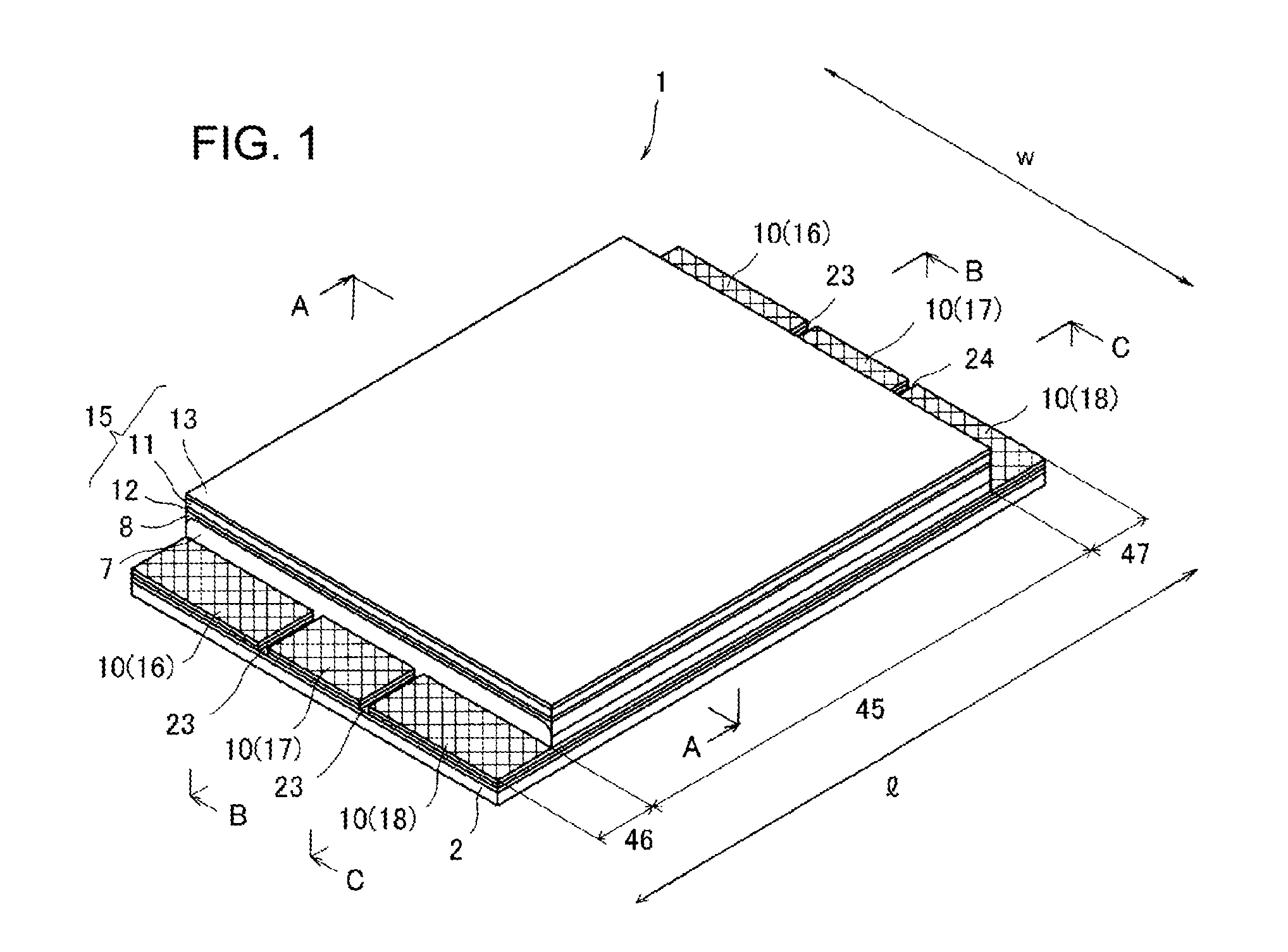
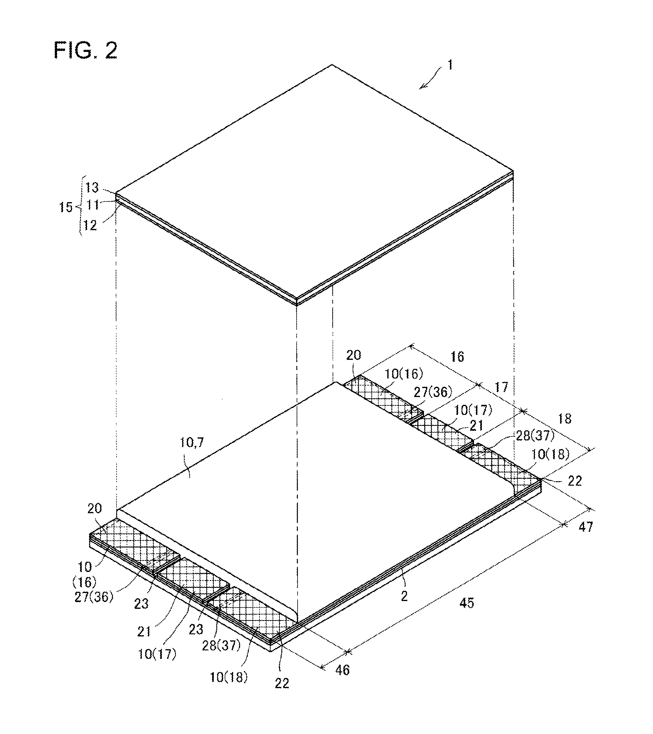
[0227]The transparent insulating substrate having a size of 80 mm by 80 mm was used as the transparent substrate on which the organic EL device is formed, and alkali-free glass (thickness of 0.7 mm) in which ITO (Indium Tin Oxide, film thickness of 150 nm) is stacked as the first electrode layer 3 on the whole surface of one of surfaces was used.

[0228]The substrate was irradiated with a laser beam having a fundamental wave (1064 nm) of YAG laser from the side of the first electrode layer 3 to form the extraction electrode isolation groove 26 having the groove width of 40 μm.

[0229]The substrate was washed with a brush using a surfactant agent, and subjected to ultrasonic cleaning using pure water. Then the substrate was dried in an oven. The substrate was moved to the vacuum evaporation apparatus, and the following materials was deposited in vacuum.

[0230]The hole-injection layer having the thickness of 10 nm was deposited on the whole surface of one of the surface of the first electr...

second example

[0240]The organic EL device was prepared in the same way as the first example except that the second inorganic sealing layer 51 is not formed and that the milled aluminum foil (thickness of 50 μm) sandwiched between the two polyethylene terephthalate (PET) resin films (thickness of 16 μm) was used as the heat-conductive sealing layer 15. The secondary sealing was performed to prepare the organic EL device including the heat-conductive sealing stacked layer structure, and the organic EL device was used as a second example.


PUM


Abstract

An organic Electro Luminescence device that equalizes heat generated in an organic EL element while preventing the intrusion of moisture. A light emitting element is covered with an inorganic sealing layer, an adhesive layer, an insulating resin film, and a metallic foil. The organic EL device includes a current carrying area located outside and along an edge of an emission area. A heat-conductive sealing stacked layer structure is formed in the current carrying area and includes the following layers in direct contact with each other in the following order: a first electrode layer extended from the emission area, auxiliary electrode layers having heat conductivity larger than that of the first electrode layer, the inorganic sealing layer, the adhesive layer, and a heat-conductive sealing layer. The heat-conductive sealing stacked layer structure having a linear shape is located near at least one side of a transparent substrate.

Description

TECHNICAL FIELD[0001]The present invention relates to an organic EL (Electro Luminescence) device. The present invention also relates to a method for manufacturing the EL device.BACKGROUND ART[0002]Nowadays, the organic EL device attracts attention as the lighting device replacing an incandescent lamp and a fluorescent lamp, and many studies are made on the organic EL device.[0003]As used herein, the organic EL device means one in which an organic EL element is stacked on transparent substrates such as a glass substrate and a transparent resin film. In the organic EL element, two electrodes in which one or both the electrodes have translucency are opposed to each other, and a light emitting layer made of an organic compound is stacked between the electrodes. The organic EL device emits light by energy of recombination of an electron and a hole that are electrically excited.[0004]That is, the organic EL device is a self-luminous device, and the organic EL device can emit the light ha...

Claims


Application Information

Patent Timeline
Patent Type & Authority Applications(United States)
IPC IPC(8): H01L51/52H01L51/56
CPCH01L51/529H01L51/56H01L51/5253H10K50/814H10K50/8423H10K50/844H10K50/87H10K50/805H10K50/824H10K59/179H10K59/1315H10K59/1795H10K71/00
Inventor WASHIO, TAKAHIRO
Owner KANEKA CORP
Why Eureka
Try Eureka