Semiconductor memory device and method of operating the same

Active Publication Date: 2015-05-14
SK HYNIX INC
View PDF13 Cites 5 Cited by
  • Summary
  • Abstract
  • Description
  • Claims
  • Application Information

AI Technical Summary

Benefits of technology

[0009]Exemplary embodiments of the present invention are directed

Problems solved by technology

A volatile memory device is unable to retain stored data when the power is turned off.
Defective blocks among the plurality of memory bloc

Method used


Image

  • Semiconductor memory device and method of operating the same
  • Semiconductor memory device and method of operating the same
  • Semiconductor memory device and method of operating the same

Examples


Example

[0022]Various exemplary embodiments of the present invention will be described in detail with reference to the accompanying drawings. The figures are provided to enable those of ordinary skill in the art to make and use the present invention according to the exemplary embodiments of the present invention.

[0023]Throughout the disclosure, reference numerals correspond directly to the like numbered parts in the various figures and embodiments of the present invention. Also, in this specification, “connected / coupled” refers to one component not only directly coupling another component but also indirectly coupling another component through an intermediate component. In addition, a singular form may include a plural form as long as it is not specifically mentioned in a sentence.

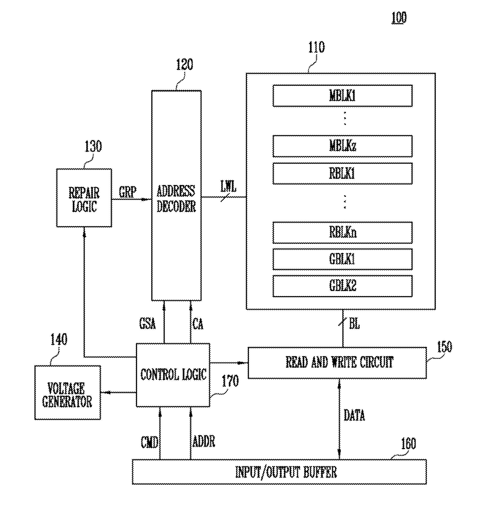
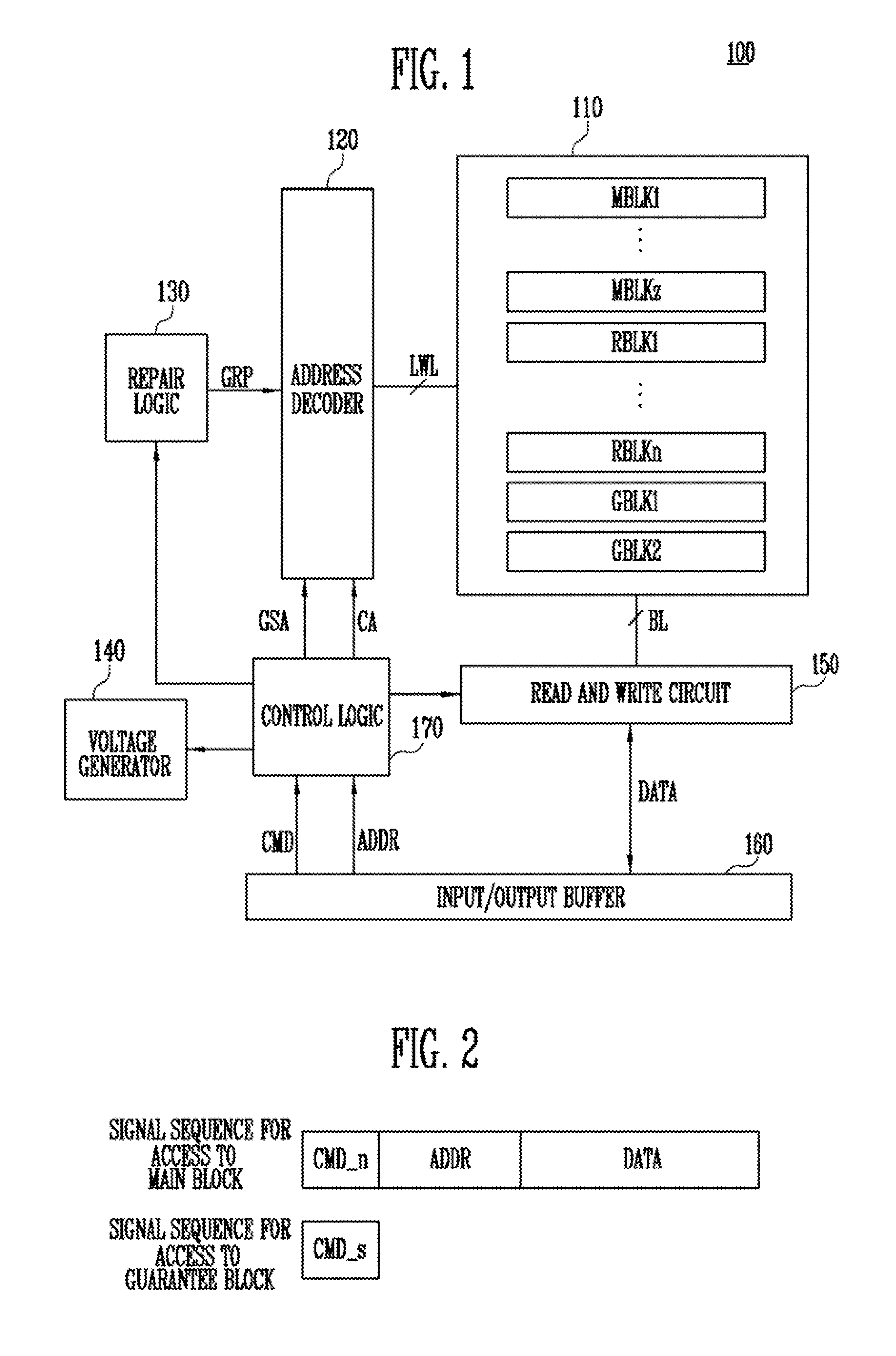
[0024]FIG. 1 is a block diagram illustrating a semiconductor memory device 100 according to an embodiment of the present invention.

[0025]Referring to FIG. 1, the semiconductor memory device 100 may include a memory...


PUM


Abstract

A semiconductor memory device includes a memory cell array having a first group of main blocks, a second group of main blocks and redundancy blocks replacing the first group of main blocks or the second group of main blocks, a repair logic suitable for enabling a replacement signal when one or more of the second group of main blocks are defective, a control logic suitable for generating an address for the second group of main blocks in response to a dedicated command for access to one or more of the second group of main blocks, and an address decoder suitable for selecting one or more of the redundancy blocks based on the address for the second group of main blocks when the replacement signal is enabled.

Description

CROSS-REFERENCE TO RELATED APPLICATION[0001]The present application claims priority to Korean patent application number 10-2013-0138532, filed on Nov. 14, 2013, the entire disclosure of which is incorporated herein in its entirety by reference.BACKGROUND[0002]1. Field of Invention[0003]Various exemplary embodiments of the present invention relate generally to an electronic device, a id more particularly, to a semiconductor memory device and a method of operating the same.[0004]2. Description of Related Art[0005]With the surge in usage of mobile information devices using semiconductor memory devices as storage media, especially smartphones and tablets, these semiconductor memory devices have gained increasing interest and importance. The emergence of a wide range of applications as well as a high-speed processor or multi-core parallelism has required increased performance and reliability of semiconductor memory devices,[0006]A semiconductor memory device is a so age device that is re...

Claims


Application Information

Patent Timeline
IPC IPC(8): G06F11/16
CPCG06F11/167G06F11/1666G06F11/20G11C16/06G11C29/14G11C16/08G11C16/10G11C16/26G11C29/72G11C29/76
Inventor LEE, SANG KYUKIM, CHANG GEUN
Owner SK HYNIX INC
Why Eureka
Try Eureka