

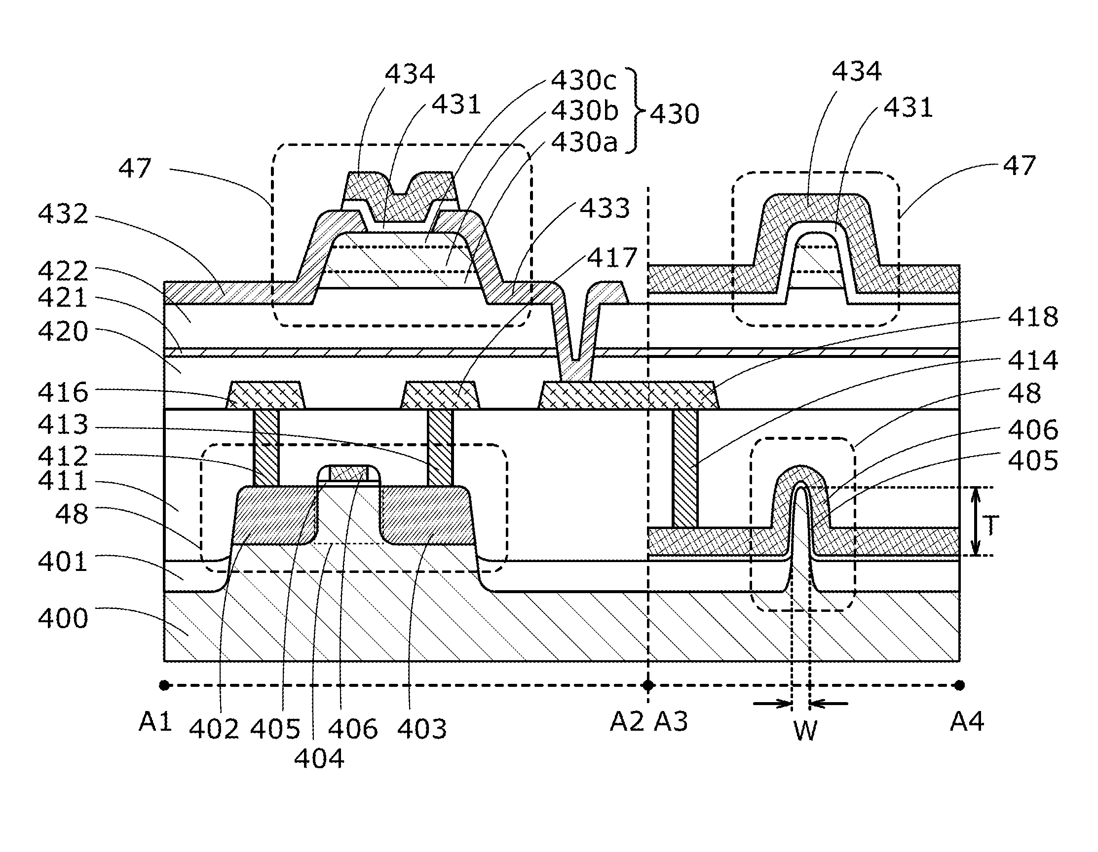
Semiconductor device
a semiconductor device and semiconductor technology, applied in the direction of semiconductor/solid-state device testing/measurement, semiconductor/solid-state device details, instruments, etc., can solve the problem of increasing the overhead of the semiconductor device including the bist circuit and the circuit to be tested, and achieve the effect of improving the quality of the operation tes
- Summary
- Abstract
- Description
- Claims
- Application Information
AI Technical Summary
Benefits of technology
Problems solved by technology
Method used
Image

Examples
example 1
Structural Example 1 of Semiconductor Device
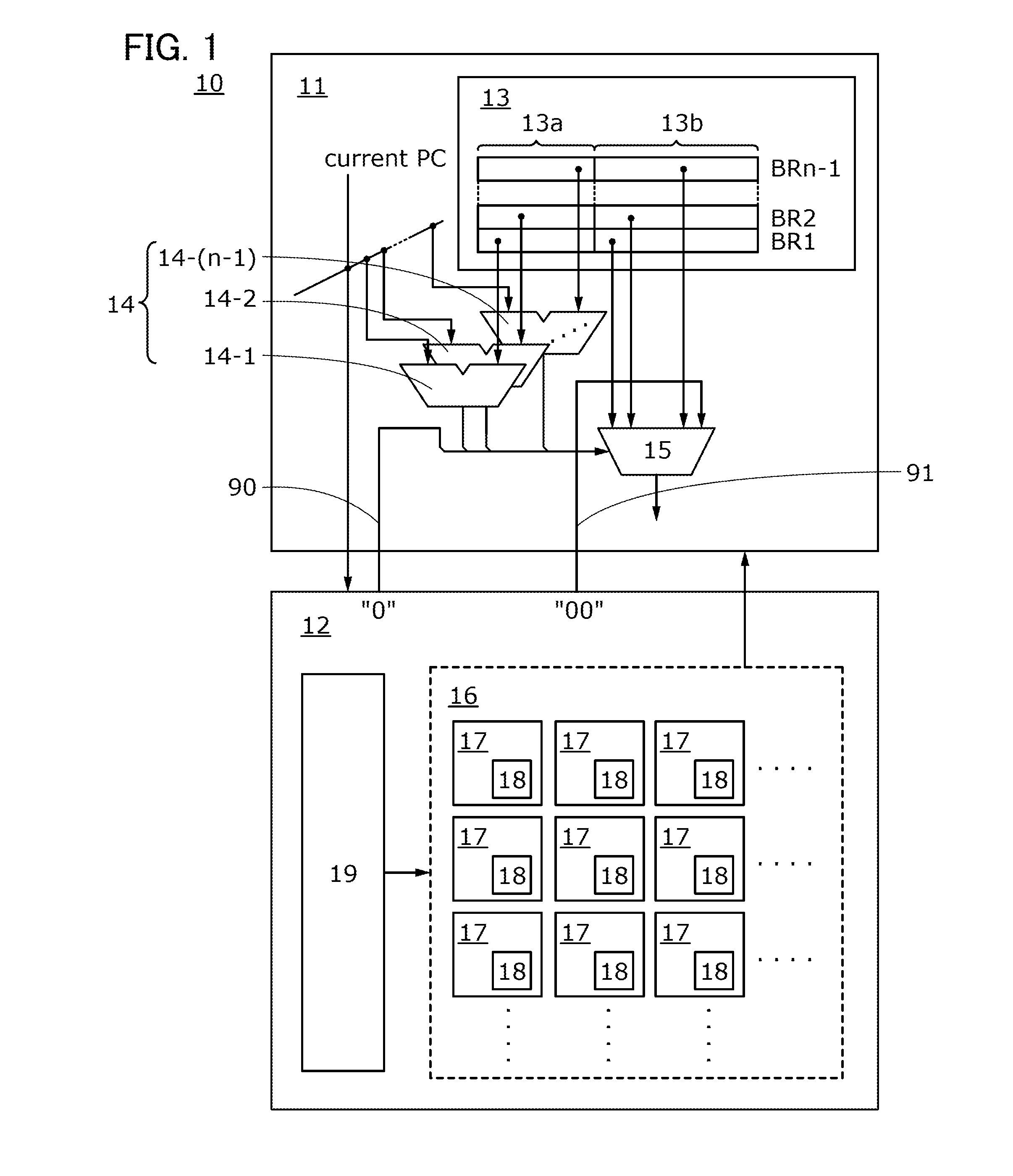
[0039]FIG. 1 illustrates a structural example of a semiconductor device 10 of one embodiment of the present invention. The semiconductor device 10 illustrated in FIG. 1 includes an integrated circuit 11 and an integrated circuit 12. The integrated circuit 11 includes a variety of logic circuits such as a sequential circuit and a combinational circuit. Each of the integrated circuits 11 and 12 includes at least two transistors, and they can be referred to as a first circuit, a second circuit, and the like or simply circuits.
[0040]The integrated circuit 11 includes a memory circuit 13, a comparator circuit 14, and a selector circuit 15. The memory circuit 13 includes a region for storing at least one pair of first data and a first address. The first data includes a history or a prediction of whether a branch condition of a branch instruction is satisfied, and the first address corresponds to the branch instruction. Specifically, FIG. 1 illus...
example 2
Structural Example 2 of Semiconductor Device
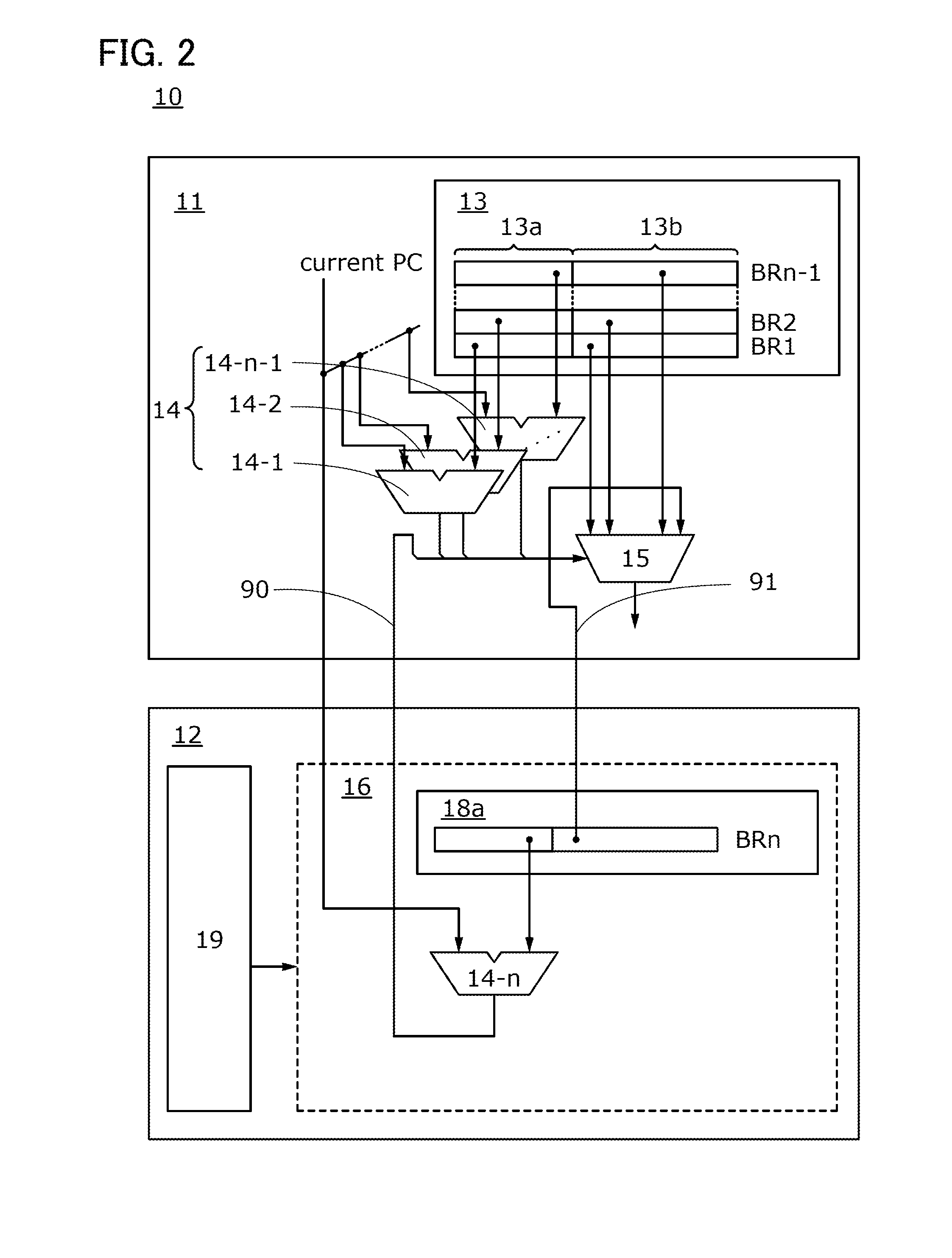
[0069]FIG. 3 schematically illustrates an operating state of the semiconductor device 10 in which the memory circuit 19 has a function of storing at least one pair BR of the first data and the first address during normal operation.
[0070]Specifically, FIG. 3 illustrates an example where a function of storing the pair BRn of the first data and the first address is added to the memory circuit 19 and the integrated circuit 12 includes the comparator circuit 14-n. The comparator circuit 14-n has a function of comparing the first address included in the pair BRn and the second address corresponding to an instruction to be executed next.
[0071]In the semiconductor device 10 in FIG. 3, the selector circuit 15 has a function of selecting the first data included in one pair BR among the n pairs BR in accordance with the results of comparison in the comparator circuits 14-1 to 14-n. For example, when the first address and the second address that are c...
PUM
 Abstract
Description
Claims
Application Information