STRUCTURE OF FinFETs

a technology of finfets and structures, applied in the direction of transistors, electrical apparatus, semiconductor devices, etc., can solve the problems of increasing leakage currents from the drain to the source, improper turning off, and unnecessary short-channel effects, so as to improve the width quantization effect, reduce the area occupied, and more linear choices for the effective width of finfets

Inactive Publication Date: 2015-05-28
NAT APPLIED RES LAB
View PDF6 Cites 35 Cited by
  • Summary
  • Abstract
  • Description
  • Claims
  • Application Information

AI Technical Summary

Benefits of technology

[0008]Another objective of the present invention is to provide a method for fabricating FinFETs, which uses an additional mask process to change the length of semiconductor fins nonuniformly so that more linear choices for the effective width of FinFETs are provided and improving the width quantization effect.
[0009]Still another objective of the present invention is to provide a method for fabricating FinFETs, which uses an additional mask process to reduce the area occupied by a single FinFET given the same layout width because a high fin has the structural characteristics of higher fin height and shorter fin width. Thereby, while fabricating electronic devices such as static random access memory (SRAM), no advanced lithography technology is required. Instead, based on increased density of layout, further device miniaturization can be performed.
[0010]A further objective of the present invention is to provide a structure of FinFETs, which has a projective taper structure at the junction between the bottom of the semiconductor fin and the insulating layer. By taking advantage of the difference in the height of semiconductor fins covered by tapers, the control of effective width can be more flexible, and thus improving the width quantization effect more effectively.
[0011]In order to achieve the objectives described above, the pres

Problems solved by technology

When planar transistors are shrunk below 20 nanometers, the gate control on the channel is reduced, resulting in increases in leakage currents from the drain to the sou

Method used


Image

  • STRUCTURE OF FinFETs
  • STRUCTURE OF FinFETs
  • STRUCTURE OF FinFETs

Examples


Embodiment Construction

[0024]In order to make the structure and characteristics as well as the effectiveness of the present invention to be further understood and recognized. the detailed description of the present invention is provided as follows along with embodiments and accompanying figures.

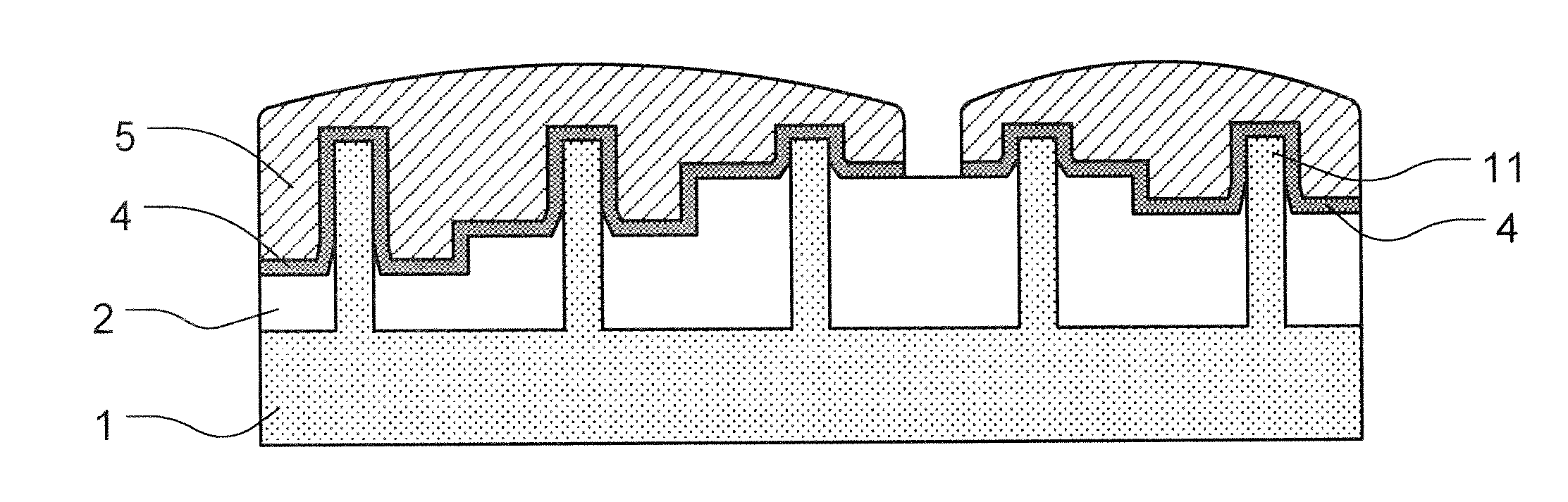
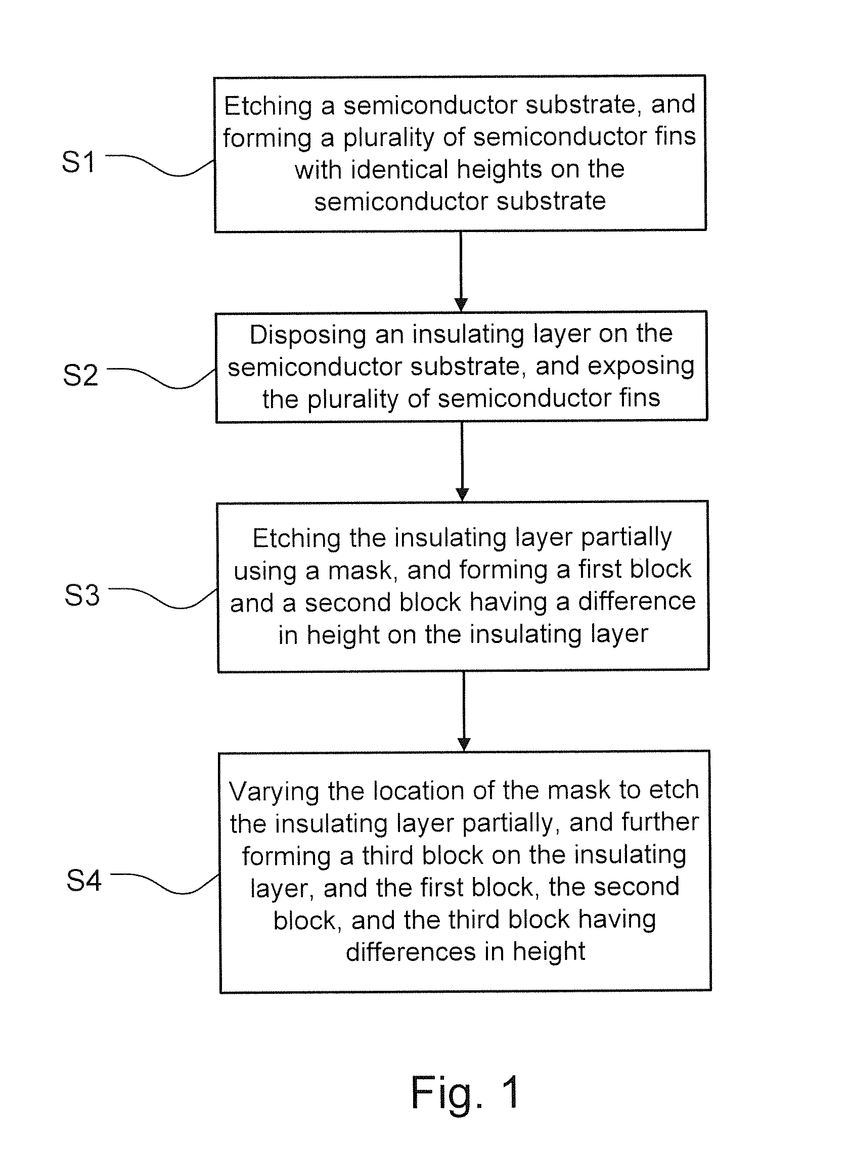
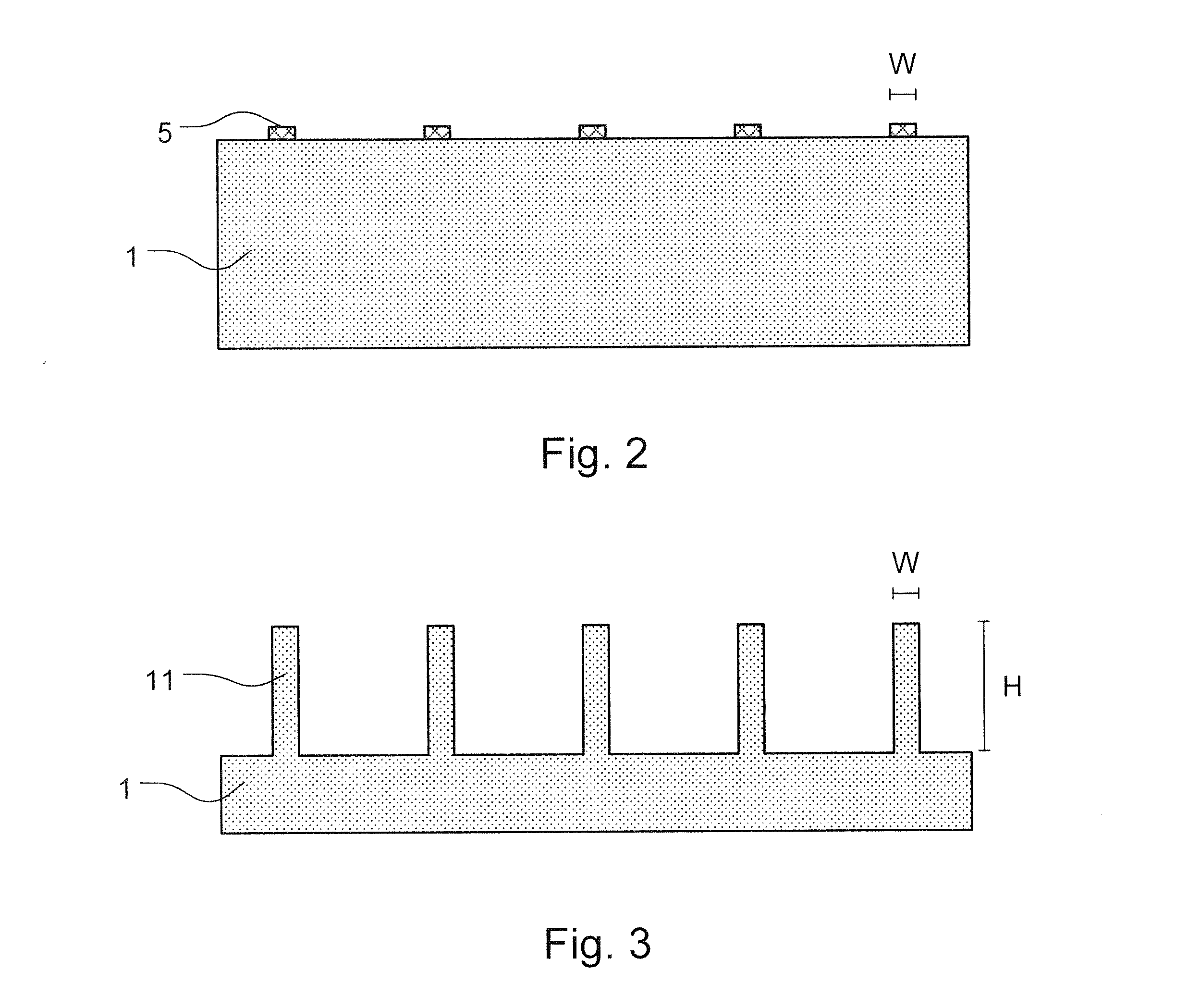
[0025]First, please refer to FIG. 1, which shows the technical characteristics of the process steps according to the present invention. The method comprises steps of:[0026]Step S1: Etching a semiconductor substrate, and forming a plurality of semiconductor fins with identical heights on the semiconductor substrate;[0027]Step S2: Disposing an insulating layer on the semiconductor substrate, and exposing the plurality of semiconductor fins;[0028]Step S3: Etching the insulating layer partially using a mask, and forming a first block and a second block having a difference in height on the insulating layer; and[0029]Step S4: Varying the location of the mask to etch the insulating layer partially, and further forming a t...


PUM


Abstract

The present invention relates to a method for fabricating FinFETs and the structure thereof. The present invention uses an additional mask to define regions forming semiconductor fins having high semiconductor-fin height. By making use of multiple etching processes of the insulating layer, structures with differences in the height of semiconductor fins are achieved. The method can be combined with current process for semiconductor-based FinFETs for overcoming effectively the problem of electron-channel-width quantization effect as well as improving the performance of FinFETs.

Description

FIELD OF THE INVENTION[0001]The present invention relates generally to a method for fabricating FinFETs and the structure thereof, and particularly to adopt an extra mask for enabling FinFETs to have different heights of semiconductor fins and reducing the width quantization effect for electron channels.BACKGROUND OF THE INVENTION[0002]The FinFET is a novel, multi-channel, and three-dimensional transistor; it improves the performance significantly and reduces the power consumption, much superior to current planar CMOS devices. In a FinFET, the gate of the device surrounds and wraps the channel, giving superior electron characteristics, providing lower threshold voltages and higher performance, and reducing leakage and dynamic power consumption.[0003]Through the particularity of fin-shaped structures of FinFETs in the three-dimensional space, the Moore's law is able to extend. FinFETs differ completely from traditional transistors, which endeavor in linear miniaturization on a plane....

Claims


Application Information

Patent Timeline
IPC IPC(8): H01L29/78H01L21/308
CPCH01L21/3083H01L29/785H01L21/823431H01L29/66795
Inventor CHEN, MIN-CHENGHO, CHIA-HUAYANG, FU-LIANG
Owner NAT APPLIED RES LAB
Why Eureka
Try Eureka