Display device

a display device and display technology, applied in the field of display devices, can solve the problems of limited irradiation area per laser light source and irradiation area per unit time, difficult to process a large-sized substrate with an insulating surface in a short time, and achieve the effects of fewer external connection terminals, high image quality, and reduced production costs

Active Publication Date: 2015-06-04
SEMICON ENERGY LAB CO LTD
View PDF6 Cites 46 Cited by
  • Summary
  • Abstract
  • Description
  • Claims
  • Application Information

AI Technical Summary

Benefits of technology

[0031]According to one embodiment of the present invention, a display device with high image quality and fewer external connection terminals can be provided.
[0032]An electronic device of one embodiment of the present invention includes a display device with high image quality and fewer external connection terminals. Accordingly, the flexibility in design such as the size of an electronic device and the position of the display device provided in the electronic device can be increased. Thus, an electronic device which is reduced in size and weight and has exc...

Problems solved by technology

A laser irradiation apparatus, which is used for a crystallization process or the like of polysilicon, has limitations on irradiation area per laser lig...

Method used


Image

  • Display device
  • Display device
  • Display device

Examples


embodiment 1

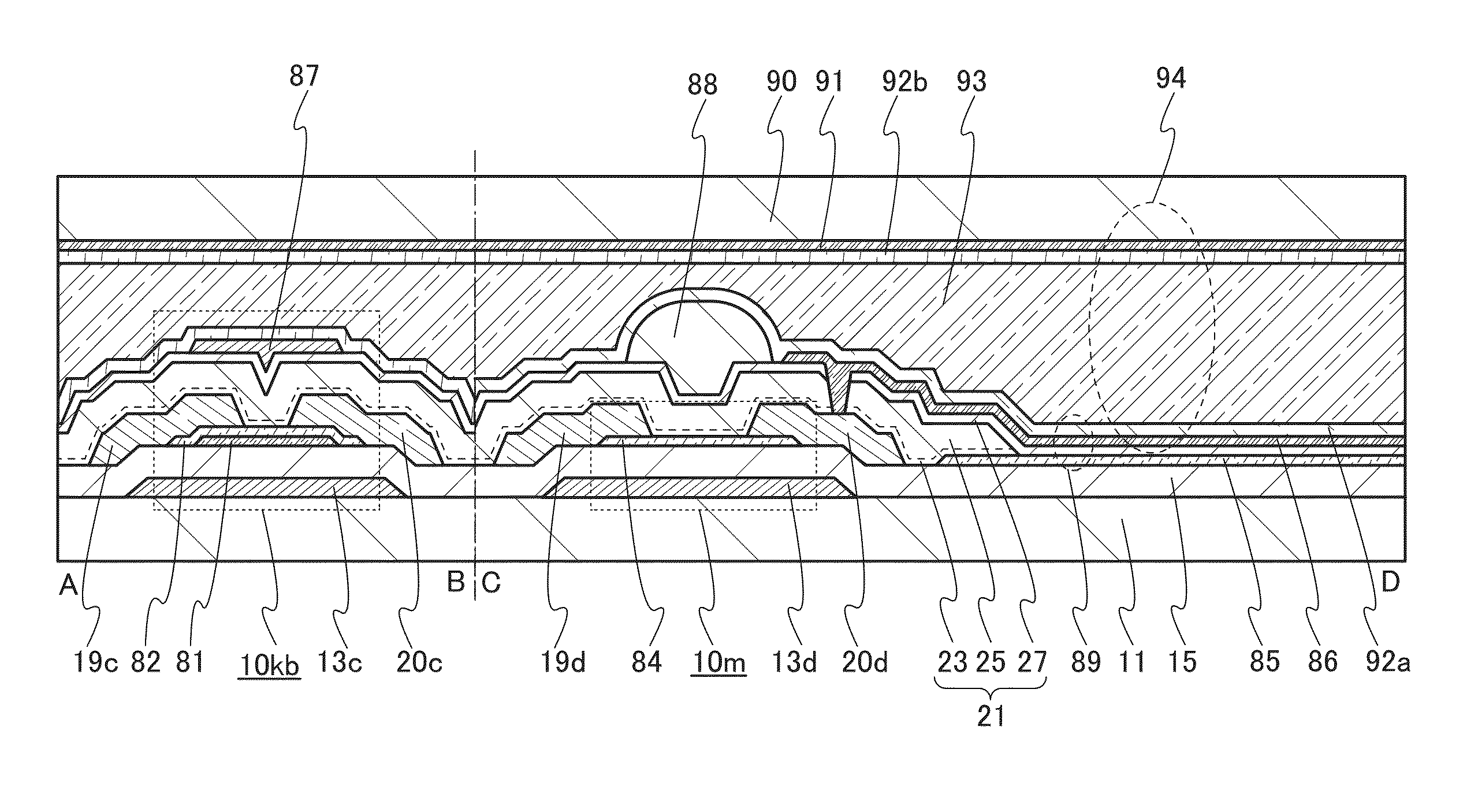
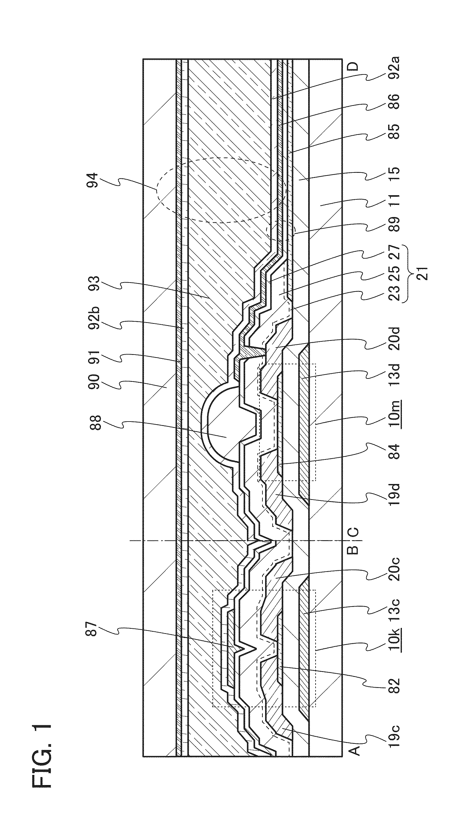
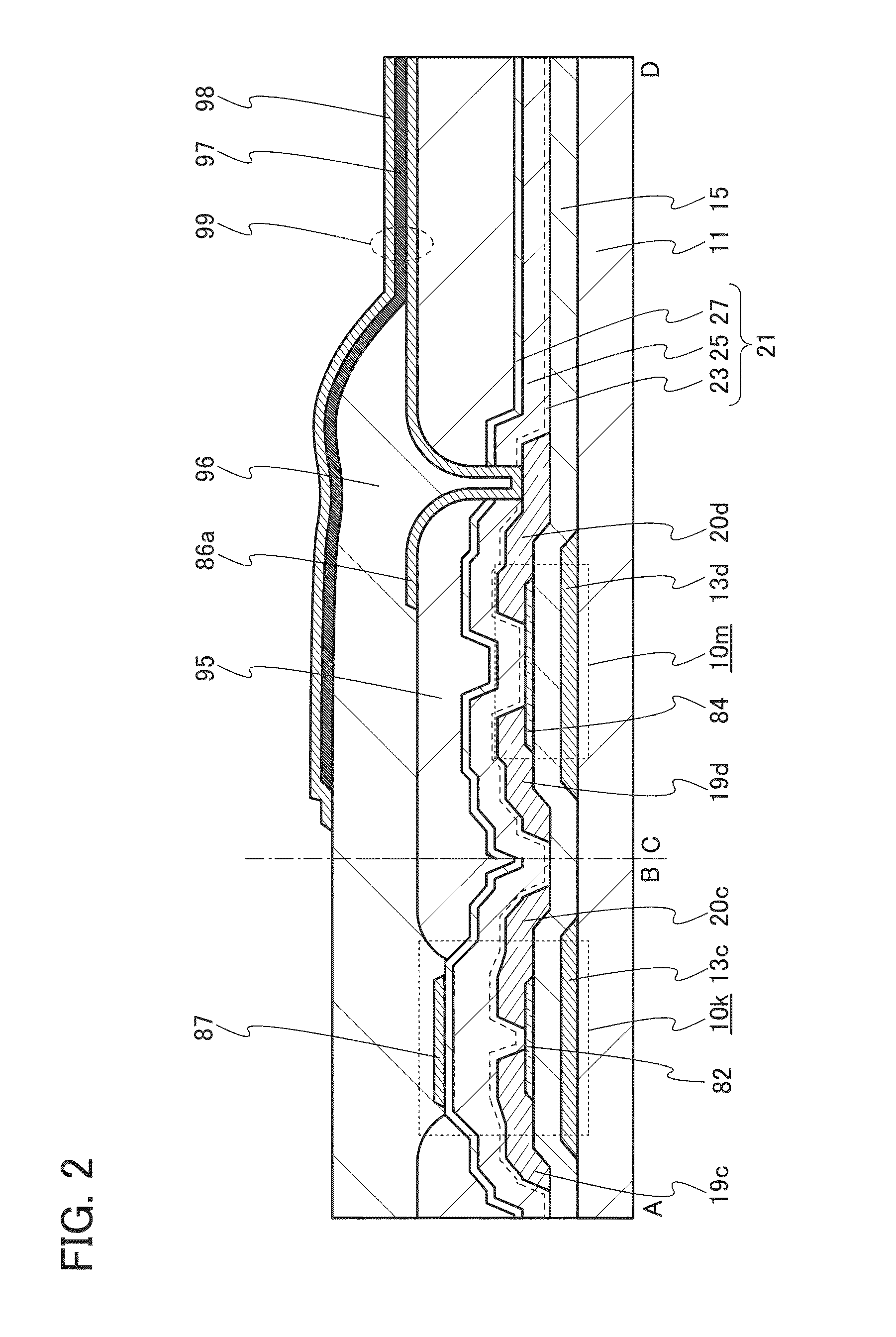
[0097]In this embodiment, a semiconductor device of one embodiment of the present invention and a method for manufacturing the semiconductor device are described with reference to drawings. Here, a liquid crystal display device and a light-emitting device are described as examples of the semiconductor device, with reference to FIG. 1, FIG. 2, FIGS. 3A to 3C, FIGS. 4A and 4B, and FIGS. 5A and 5B. In this embodiment, the semiconductor devices each include a first transistor and a second transistor, which include oxide semiconductor films with different structures.

[0098]First, a liquid crystal display device is described.

[0099]FIG. 1 is a cross-sectional view of the liquid crystal display device; a transistor formed in a driver circuit portion is shown in a cross section A-B, and a transistor formed in a pixel portion is shown in a cross section C-D.

[0100]A transistor 10k shown in the cross section A-B in FIG. 1 includes a gate electrode 13c over a substrate 11, a gate insulating film ...

embodiment 2

[0236]In this embodiment, a structure example of a display device of one embodiment of the present invention is described.

[0237]FIG. 6A is a top view of the display device of one embodiment of the present invention. FIG. 6B is a circuit diagram illustrating a pixel circuit that can be used in the case where a liquid crystal element is used in a pixel in the display device of one embodiment of the present invention. FIG. 6C is a circuit diagram illustrating a pixel circuit that can be used in the case where an organic EL element is used in a pixel in the display device of one embodiment of the present invention.

[0238]The transistor in the pixel portion can be formed in accordance with the above embodiment. Further, the transistor can be easily formed as an n-channel transistor, and thus, part of a driver circuit that can be formed using an n-channel transistor is formed over the same substrate as the transistor in the pixel portion. Thus, the pixel portion and the driver circuit are ...

embodiment 3

[0265]In this embodiment, one embodiment that can be applied to the oxide semiconductor film in any of the transistors included in the semiconductor device described in Embodiment 1 is described.

[0266]The oxide semiconductor film may include one or more of the following: an oxide semiconductor having a single-crystal structure (hereinafter referred to as a single-crystal oxide semiconductor); an oxide semiconductor having a polycrystalline structure (hereinafter referred to as a polycrystalline oxide semiconductor); an oxide semiconductor having a microcrystalline structure (hereinafter referred to as a microcrystalline oxide semiconductor), and an oxide semiconductor having an amorphous structure (hereinafter referred to as an amorphous oxide semiconductor). Further, the oxide semiconductor film may be formed using a CAAC-OS film. Furthermore, the oxide semiconductor film may include an amorphous oxide semiconductor and an oxide semiconductor having a crystal grain. Described below...


PUM


Abstract

To provide a display device in which plural kinds of circuits are formed over one substrate and plural kinds of transistors corresponding to characteristics of the plural kinds of circuits are provided. The display device includes a pixel portion and a driver circuit that drives the pixel portion over one substrate. The pixel portion includes a first transistor including a first oxide semiconductor film. The driver circuit includes a second transistor including a second oxide semiconductor film. The first oxide semiconductor film and the second oxide semiconductor film are formed over one insulating surface. A channel length of the first transistor is longer than a channel length of the second transistor. The channel length of the first transistor is greater than or equal to 2.5 micrometer.

Description

TECHNICAL FIELD[0001]The present invention relates to an object, a method, or a manufacturing method. In addition, the present invention relates to a process, a machine, manufacture, or a composition of matter. In particular, the present invention relates to a semiconductor device, a display device, a light-emitting device, a power storage device, a memory device, a driving method thereof, or a manufacturing method thereof. Furthermore, in particular, the present invention relates to a semiconductor device including a field-effect transistor.[0002]In this specification and the like, a semiconductor device generally means a device that can function by utilizing semiconductor characteristics. A semiconductor element such as a transistor, a semiconductor circuit, an arithmetic device, and a memory device are each one embodiment of a semiconductor device. An imaging device, a display device, a liquid crystal display device, a light-emitting device, an electro-optical device, a power gen...

Claims


Application Information

Patent Timeline
IPC IPC(8): G02F1/1368H01L27/12G02F1/133G02F1/1362G02F1/1333
CPCG02F1/1368G02F1/136286H01L27/1225G02F1/13306G02F1/136277G02F1/133345H01L29/78648H01L29/78696H01L27/1251H01L29/7869H10K59/1213H10K59/1201H01L27/1248
Inventor YAMAZAKI, SHUNPEIOKAZAKI, KENICHIKATAYAMA, MASAHIRO
Owner SEMICON ENERGY LAB CO LTD
Why Eureka
Try Eureka