Method of collective manufacture of leds and structure for collective manufacture of leds

Inactive Publication Date: 2015-06-04
S O I TEC SILICON ON INSULATOR THECHNOLOGIES
View PDF14 Cites 41 Cited by
  • Summary
  • Abstract
  • Description
  • Claims
  • Application Information

AI Technical Summary

Benefits of technology

[0016]Thus, the inventive method makes it possible to collectively form n-type contact pads and p-type contact pads for the whole of the elemental structures present on the substrate. The number of operations required to form the contact pads is here considerably fewer in relation to the prior art wherein contact pads are formed independently on each elemental structure. One thus has a substrate or

Problems solved by technology

Although carrying out these operations individually allows good control of the precision of the LED manufacturing process, it mu

Method used


Image

  • Method of collective manufacture of leds and structure for collective manufacture of leds
  • Method of collective manufacture of leds and structure for collective manufacture of leds
  • Method of collective manufacture of leds and structure for collective manufacture of leds

Examples


Embodiment Construction

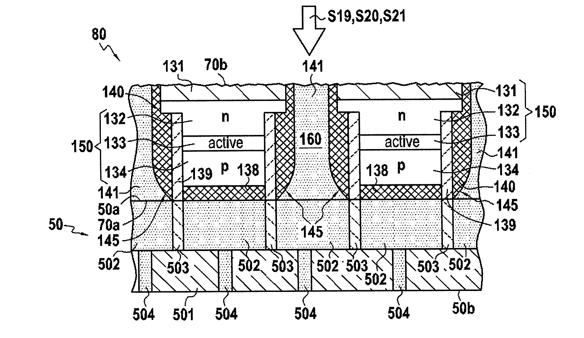
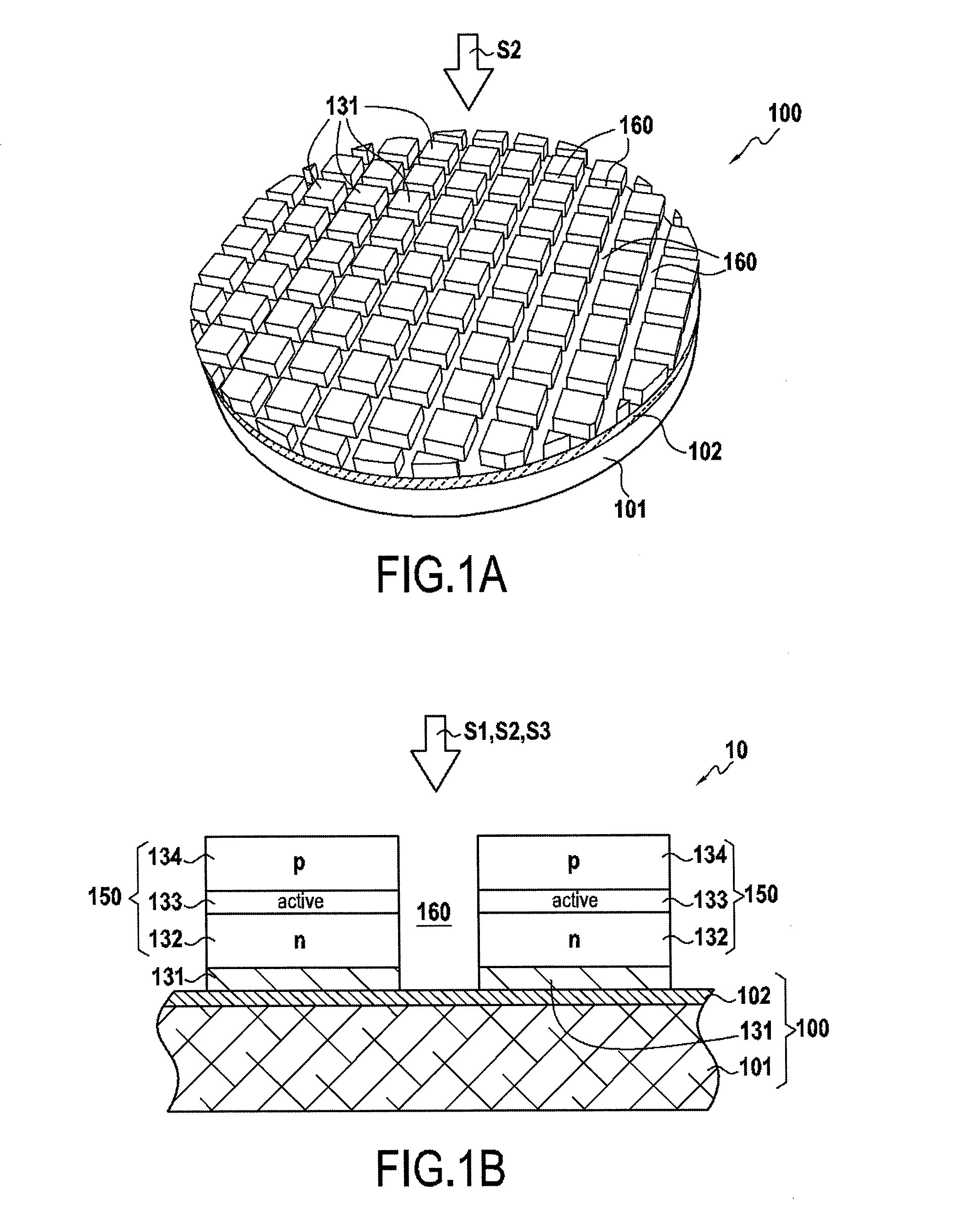
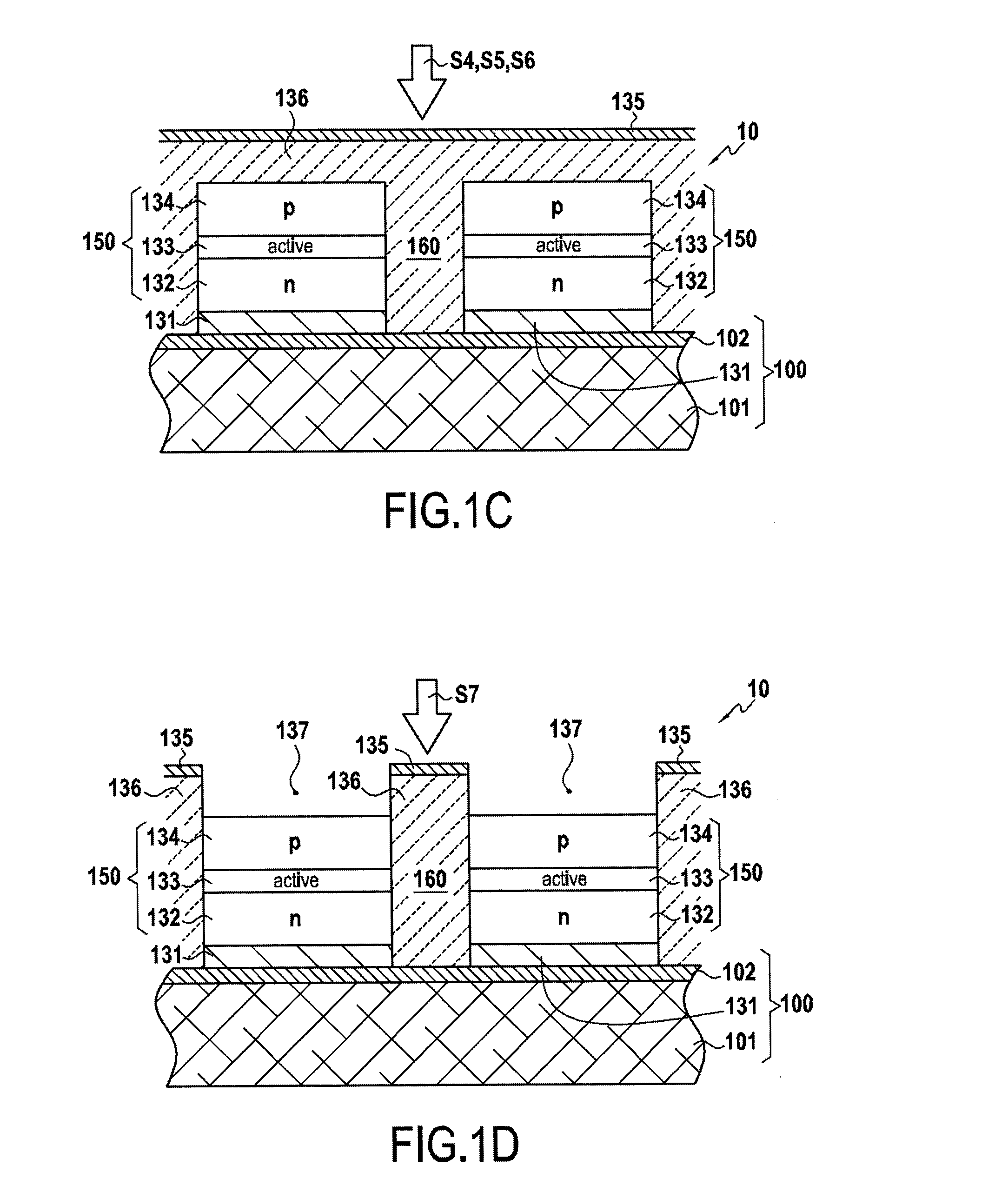
[0052]This disclosure applies to the collective manufacture of light-emitting diode (LED) devices. As explained in detail below, the disclosure allows the collective manufacture of LED devices on a plate, each comprising at least one or more elemental LED structures that, at different stages of the process, are further provided with one or more of the following elements:[0053]p-type contacts,[0054]n-type contacts,[0055]a final substrate provided with vertical electronic connections (vias) for access to the contacts, the final substrate being further able to be provided with electronic circuits,[0056]a light-converting material layer,[0057]microstructures, in particular, optical microstructures.

[0058]All of the elements mentioned above can be prepared collectively as in the example described below, i.e., during the same operations carried out on the whole of the elemental LED structures present on the plate. However, if need be, the LED devices can be cut out at an intermediate stage...


PUM


Abstract

The disclosure relates to a method of collective manufacturing of light-emitting diode (LED) devices comprising formation of elemental structures, each comprising an n-type layer, an active layer and a p-type layer, the method comprising: —reduction of the lateral dimensions of part of each elemental LED structure; —formation of a portion of insulating material on the sides of the elemental structures;—formation of n-type electrical contact pads and p-type electrical contact pads; —deposition of a conductive material layer; on the elemental structures and polishing of the conductive material layer; and—bonding by molecular adhesion of a second substrate on the polished surface of the structure.

Description

CROSS-REFERENCE TO RELATED APPLICATIONS[0001]This application is a national phase entry under 35 U.S.C. §371 of International Patent Application PCT / EP2013 / 062658, filed Jun. 18, 2013, designating the United States of America and published in English as International Patent Publication WO 2013 / 189949 A1 on Dec. 27, 2013, which claims the benefit under Article 8 of the Patent Cooperation Treaty and under 35 U.S.C. §119(e) to French Patent Application Serial Nos. 1255931 and 1255934, both filed Jun. 22, 2012, the disclosure of each of which is hereby incorporated herein in its entirety by this reference.TECHNICAL FIELD[0002]This disclosure relates to the manufacture of light-emitting diodes (LEDs).BACKGROUND[0003]LEDs are generally manufactured from elemental structures corresponding to a stack of layers comprising at least one n-type layer or region, a p-type layer or region and an active layer disposed between the n-type and p-type layers. These elemental LED structures can be forme...

Claims


Application Information

Patent Timeline
IPC IPC(8): H01L27/15H01L33/12H01L33/00H01L33/62
CPCH01L27/153H01L33/62H01L2933/0066H01L33/005H01L33/12H01L31/1892H01L33/20H01L33/385H01L2933/0016H01L2933/0033H01L31/02008H01L31/075Y02E10/548H01L27/156H01L33/0095H01L33/0093
Inventor GUENARD, PASCAL
Owner S O I TEC SILICON ON INSULATOR THECHNOLOGIES
Why Eureka
Try Eureka