Display substrates, methods of manufacturing the same and display devices including the same

a technology of display substrates and substrates, which is applied in the direction of identification means, instruments, semiconductor devices, etc., can solve the problems of damage to the active layer, and achieve the effect of reducing the amount of etching for providing the contact structure and thinness of the layer structure on the data pad

Inactive Publication Date: 2015-06-11
SAMSUNG DISPLAY CO LTD
View PDF1 Cites 16 Cited by
  • Summary
  • Abstract
  • Description
  • Claims
  • Application Information

AI Technical Summary

Benefits of technology

[0031]According to exemplary embodiments, a gate insulation layer may be etched using a gate electrode as an etching mask to expose a peripheral portion of an active layer. The etching process for the gate insulation layer may include two processes to prevent a damage of the active layer. Additionally, a buffer layer disposed under the active layer and covering a data pad may also be partially etched together with the gate insulation layer. Therefore, when contact structures electrically connected to the peripheral portion of the active layer and the data pad are provided, a thickness of a layer structure disposed on the data pad may be decreased so that an etching amount for providing the contact structure may be effectively reduced. Accordingly, an etching damage occurring at a portion of the active layer in contact with the contact structure may be effectively prevented.

Problems solved by technology

When an insulation layer is etched, an active layer may be damaged during an etching process for the insulation layer.

Method used


Image

  • Display substrates, methods of manufacturing the same and display devices including the same
  • Display substrates, methods of manufacturing the same and display devices including the same
  • Display substrates, methods of manufacturing the same and display devices including the same

Examples


experimental example

Evaluation on Damages of an Active Layer

example

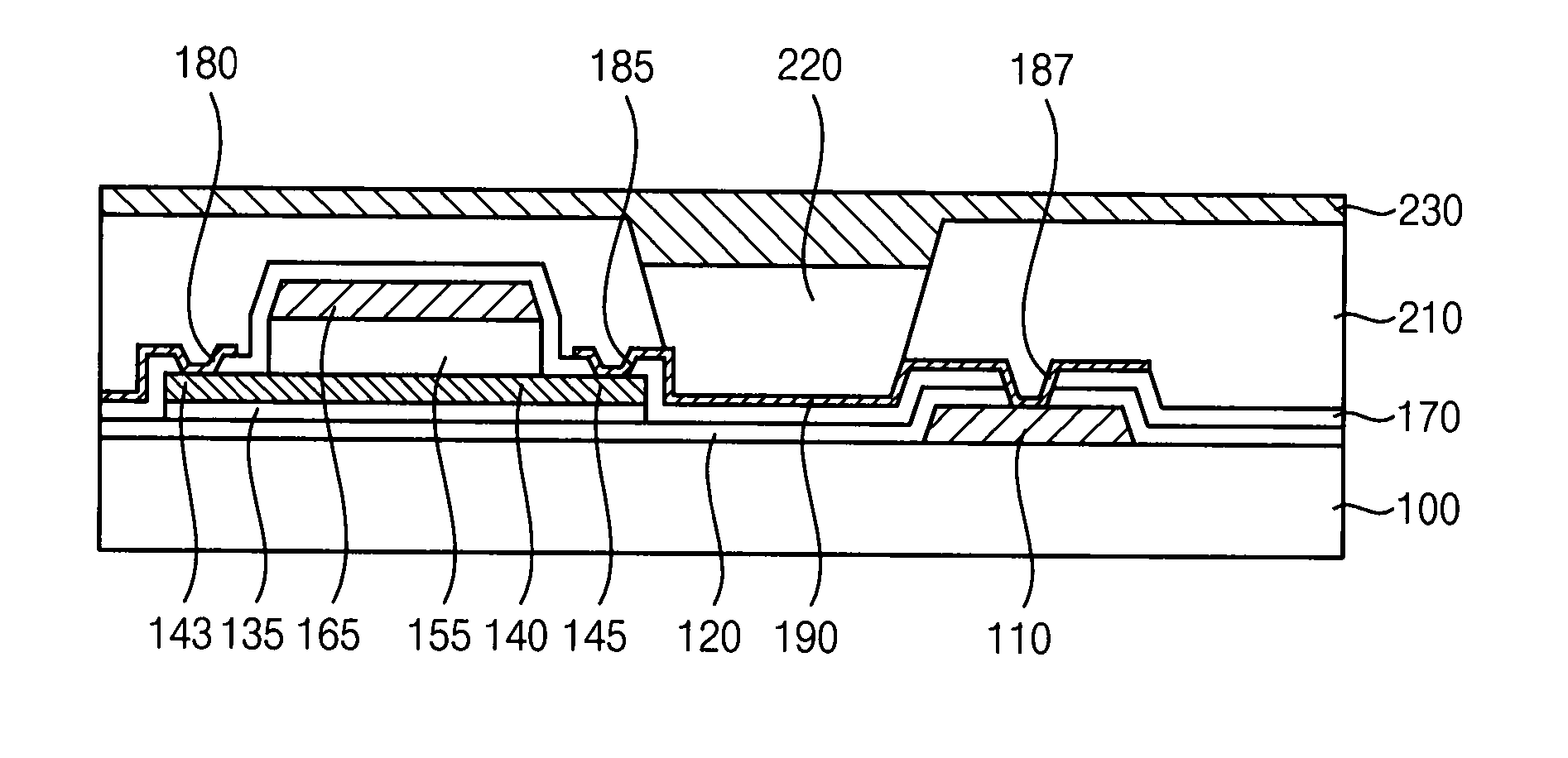
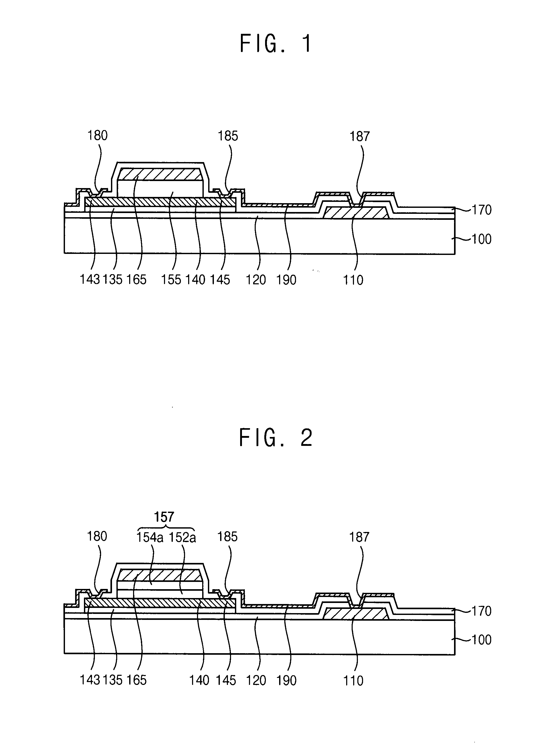
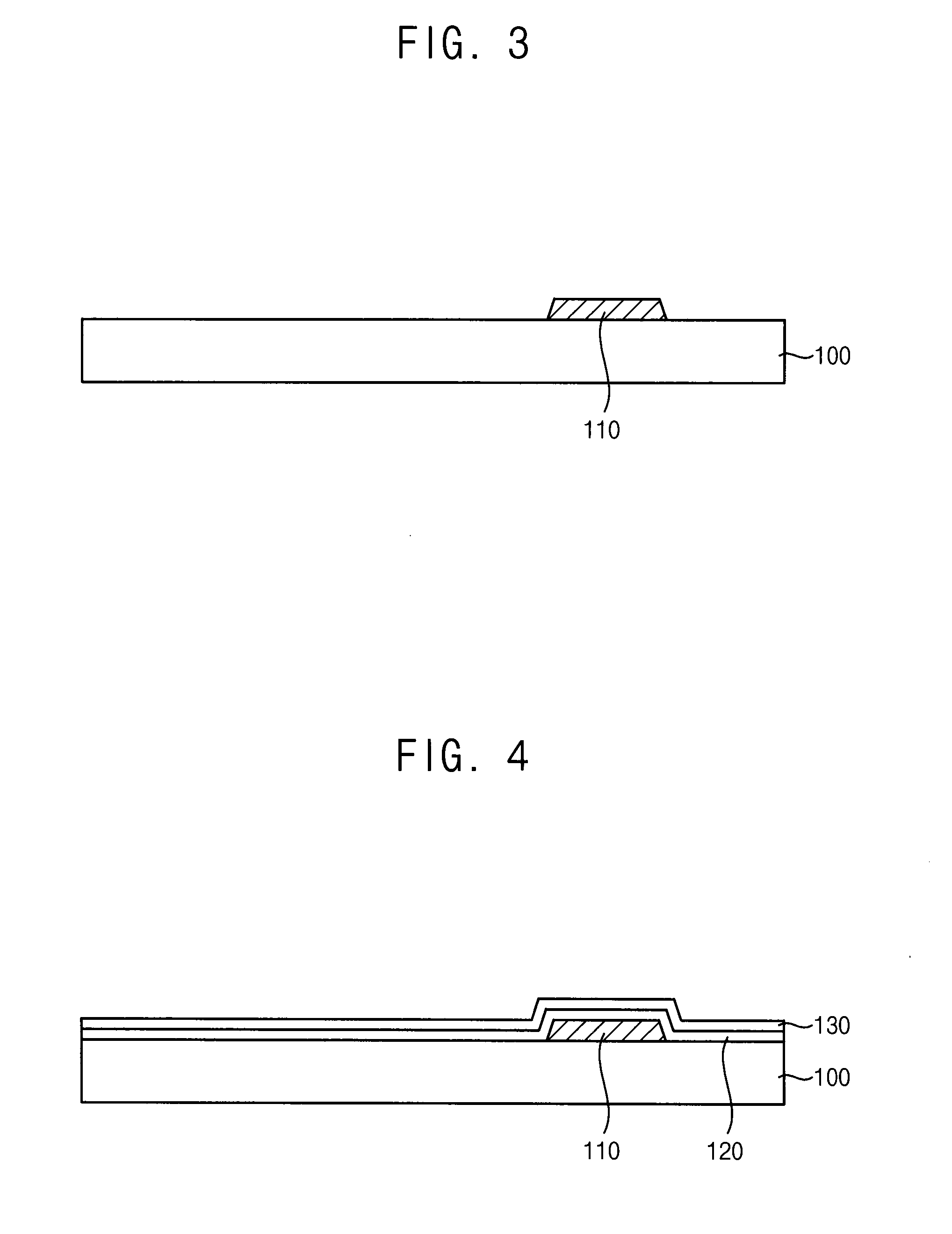
[0140]A display substrate was manufactured by performing processes substantially the same as or similar to those illustrated with reference to FIGS. 3 to 10. Specifically, a data pad 110 was disposed on a base substrate 100, and then a first buffer layer 120 and a second buffer layer 130 covering the data pad 110 were provided using silicon nitride and silicon oxide, respectively. Thicknesses of the first buffer layer 120 and the second buffer layer 130 were 1000 angstrom (Å) and 500 Å, respectively. An active layer 140 was disposed on the second buffer layer 130 using IGZO. A thickness of the active layer was 500 Å.

[0141]A gate insulation layer 150 having a thickness of 2000 Å was disposed on the second buffer layer 130 using silicon oxide. A gate electrode 165 having a double-layered structure of Ti / Cu layers was disposed on the gate insulation layer 150. A thickness of the gate electrode 165 was 3000 Å. A first etching process was performed to partially etch the gate insulation l...


PUM


Abstract

A display substrate includes a data pad on a base substrate, a first buffer layer which covers the data pad, a second buffer layer pattern which is disposed on the first buffer layer and separated from the data pad in a plan view, an active layer on the second buffer layer pattern, a gate insulation layer pattern on the active layer, both ends of the active layer exposed by the gate insulation layer pattern, and a gate electrode on the gate insulation layer pattern.

Description

[0001]This application claims priority to Korean Patent Application No. 10-2013-0150347 filed on Dec. 5, 2013, and all the benefits accruing therefrom under 35 U.S.C. §119, the entire disclosure of which is incorporated by reference herein.BACKGROUND[0002]1. Field[0003]Exemplary embodiments relate to display substrates, methods of manufacturing the same and display devices including the same. More particularly, exemplary embodiments relate to top-gate type display substrates, methods of manufacturing the same and display devices including the same.[0004]2. Description of the Related Art[0005]A display device including an organic light emitting display (“OLED”) device or a liquid crystal display (“LCD”) device, for example, may include a light emitting structure having an organic light emitting layer or a liquid crystal layer on a display substrate.[0006]The display substrate may include a switching device such as a thin film transistor (“TFT”) and a wiring structure such as a data l...

Claims


Application Information

Patent Timeline
Patent Type & Authority Applications(United States)
IPC IPC(8): H01L27/12
CPCH01L27/1218H01L27/1262H01L27/124G09F9/30G09F9/33H01L29/786
Inventor KIM, JAE-NEUNGJEONG, YU-GWANGCHOI, SHIN-ILKIM, DAE-HOCHA, MYOUNG-GEUNKIM, SANG-GABSON, JUNG-HA
Owner SAMSUNG DISPLAY CO LTD
Why Eureka
Try Eureka