Inspection appratus and inspection method

a technology of inspection apparatus and inspection method, which is applied in the field of inspection apparatus of semiconductor devices, can solve the problems of troublesome optimization work and increase the cost of apparatus, and achieve the effect of enhancing the intensity of electromagnetic waves

Inactive Publication Date: 2015-06-11
DAINIPPON SCREEN MTG CO LTD +1
View PDF14 Cites 23 Cited by
  • Summary
  • Abstract
  • Description
  • Claims
  • Application Information

AI Technical Summary

Benefits of technology

[0012]The internal electric field can easily be enhanced in the inspection object by sort-circuiting the anode and the cathode. Therefore, because the intensity of the emitted electromagnetic wave can be enhanced, the S / N ratio of the detected electromagnetic wave can be improved.
[0014]The internal electric field can easily be enhanced with respect to the inspection object including the p-type semiconductor and the n-type semiconductor.
[0016]The intensity of the emitted electromagnetic wave can be enhanced without applying the reverse bias voltage with respect to the multi-junction type solar cell. Therefore, the breakage of the solar cell can be constrained.
[0021]Therefore, an object of the present invention is to provide a technology of easily enhancing the intensity of the electromagnetic wave emitted from the inspection object.

Problems solved by technology

However, in the conventional technology, it is necessary to provide a circuit or light source applying the reverse bias voltage in order to improve the S / N ratio of the electromagnetic wave intensity, which results in an increase of apparatus cost and a troublesome work to optimize a condition.

Method used


Image

  • Inspection appratus and inspection method
  • Inspection appratus and inspection method
  • Inspection appratus and inspection method

Examples


Embodiment Construction

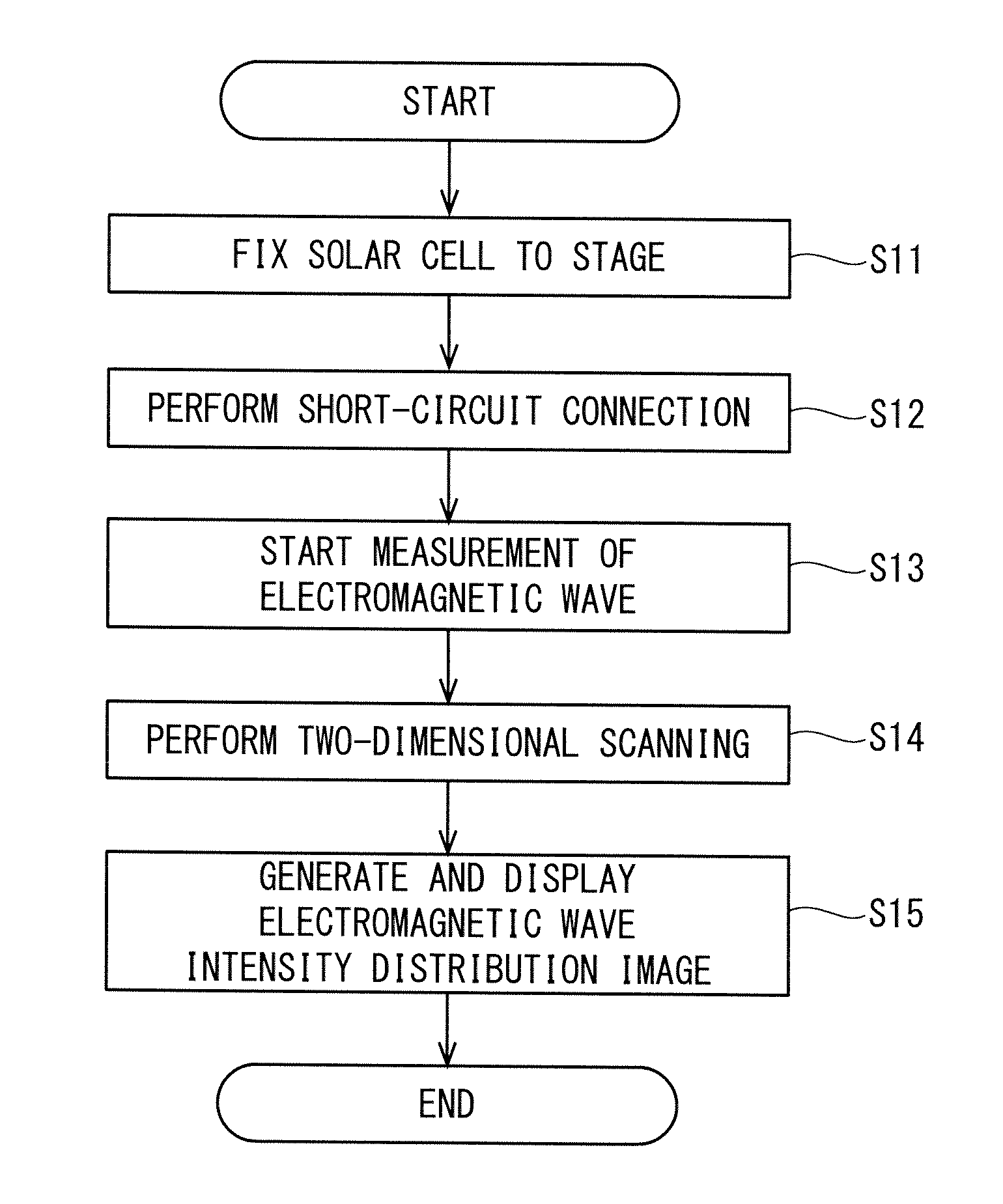
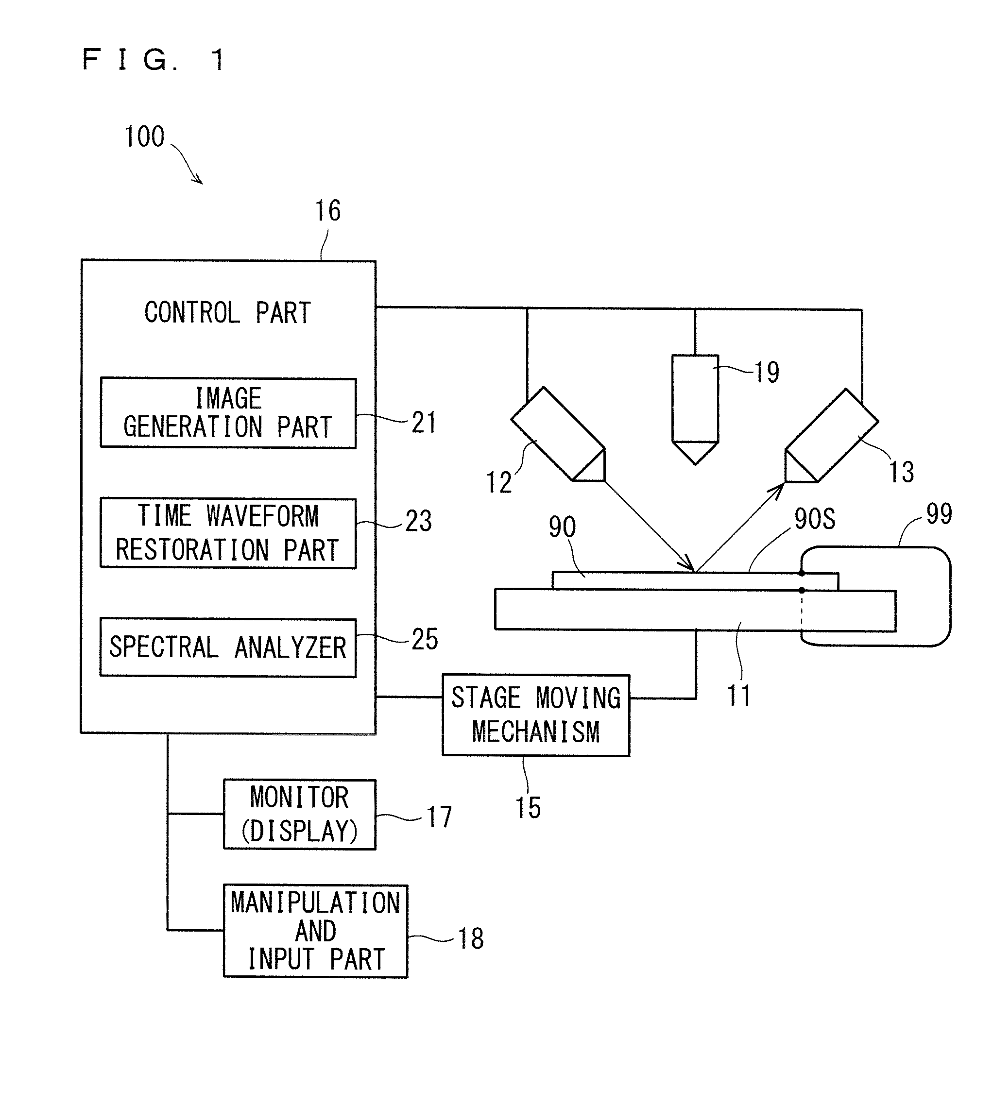
[0033]Hereinafter, preferred embodiments of the present invention will be described below with reference to the accompanying drawings. In the drawings, for the sake of easy understanding, a size of each unit or the number of units is exaggerated or simplified as needed basis. The components of the preferred embodiment are described only by way of example, but the present invention is not limited to the preferred embodiment.

1. Preferred Embodiment

1.1. Configuration and Function

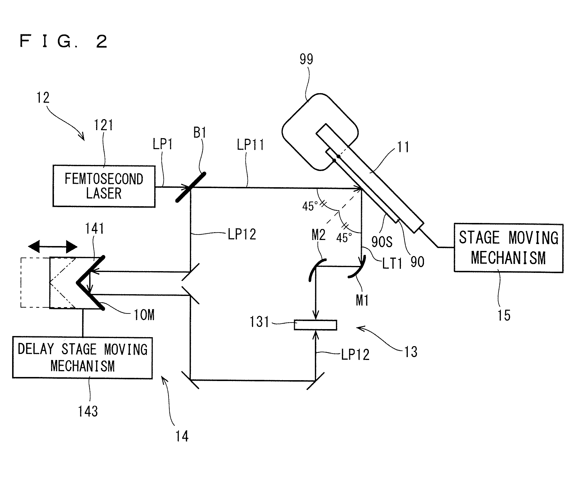
[0034]FIG. 1 is a schematic diagram illustrating a configuration of an inspection apparatus 100 according to a preferred embodiment. FIG. 2 is a schematic diagram illustrating configurations of an irradiation part 12, a detection part 13, and a delay part 14 that are included in the inspection apparatus 100.

[0035]The inspection apparatus 100 irradiates an inspection object that is of a semiconductor device or a photo device with pulse light, and detects an electromagnetic wave (for example, a terahertz wave hav...


PUM


Abstract

An inspection apparatus inspects a solar cell. The inspection apparatus includes: a short-circuiting element that electrically connects an anode as a p-type semiconductor layer and a cathode as an n-type semiconductor layer of the solar cell to short-circuit the solar cell; an irradiation part that irradiates the solar cell short-circuited by the short-circuiting element with pulse light; and a detection part that detects an electromagnetic wave emitted from the solar cell in response to the irradiation of the solar cell with pulse light from the irradiation part.

Description

BACKGROUND OF THE INVENTION[0001]1. Field of the Invention[0002]The present invention relates to a technology of inspecting a semiconductor device, a photo device, or a light emitting device.[0003]2. Description of the Background Art[0004]Nowadays, a technical development that visualizes dynamic behaviors such as generation, acceleration, and recombination of photocarriers (particularly, electrons), what is called carrier dynamics has been expected in fields of a semiconductor and a photo device, particularly in the field of a solar cell. An observation system used in time regions of femtosecond to picosecond is required in the carrier dynamics.[0005]There is performed research and development on an observation system in which an electromagnetic wave (terahertz wave, 1012Hz) in a terahertz region is used. The electromagnetic wave in the terahertz region has high transmissivity like a radio wave and rectilinear traveling property like light, and practical use of the electromagnetic w...

Claims


Application Information

Patent Timeline
Patent Type & Authority Applications(United States)
IPC IPC(8): H02S50/15G01R31/265
CPCG01R31/2656H02S50/15Y02E10/50
Inventor NAKANISHI, HIDETOSHIITO, AKIRAKAWAYAMA, IWAOTONOUCHI, MASAYOSHI
Owner DAINIPPON SCREEN MTG CO LTD
Why Eureka
Try Eureka