

Methods for inspecting semiconductor wafers
a technology of semiconductor wafers and inspection methods, applied in the direction of individual semiconductor device testing, fluorescence/phosphorescence, instruments, etc., can solve the problems of metal contact structure breakage, pv cell failure, undetectable low efficiency
- Summary
- Abstract
- Description
- Claims
- Application Information
AI Technical Summary
Benefits of technology
Problems solved by technology
Method used
Image

Examples
Embodiment Construction
[0068]Preferred embodiments of the invention will now be described, by way of example only, with reference to the accompanying drawings.
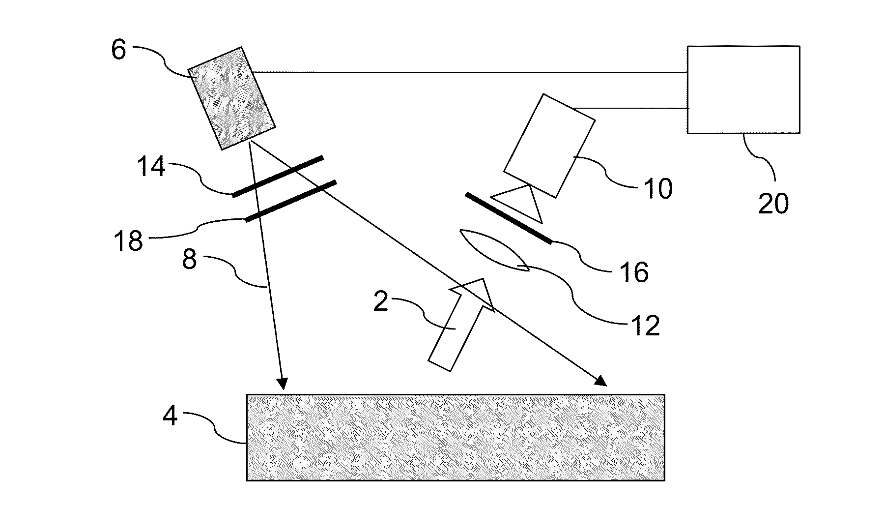
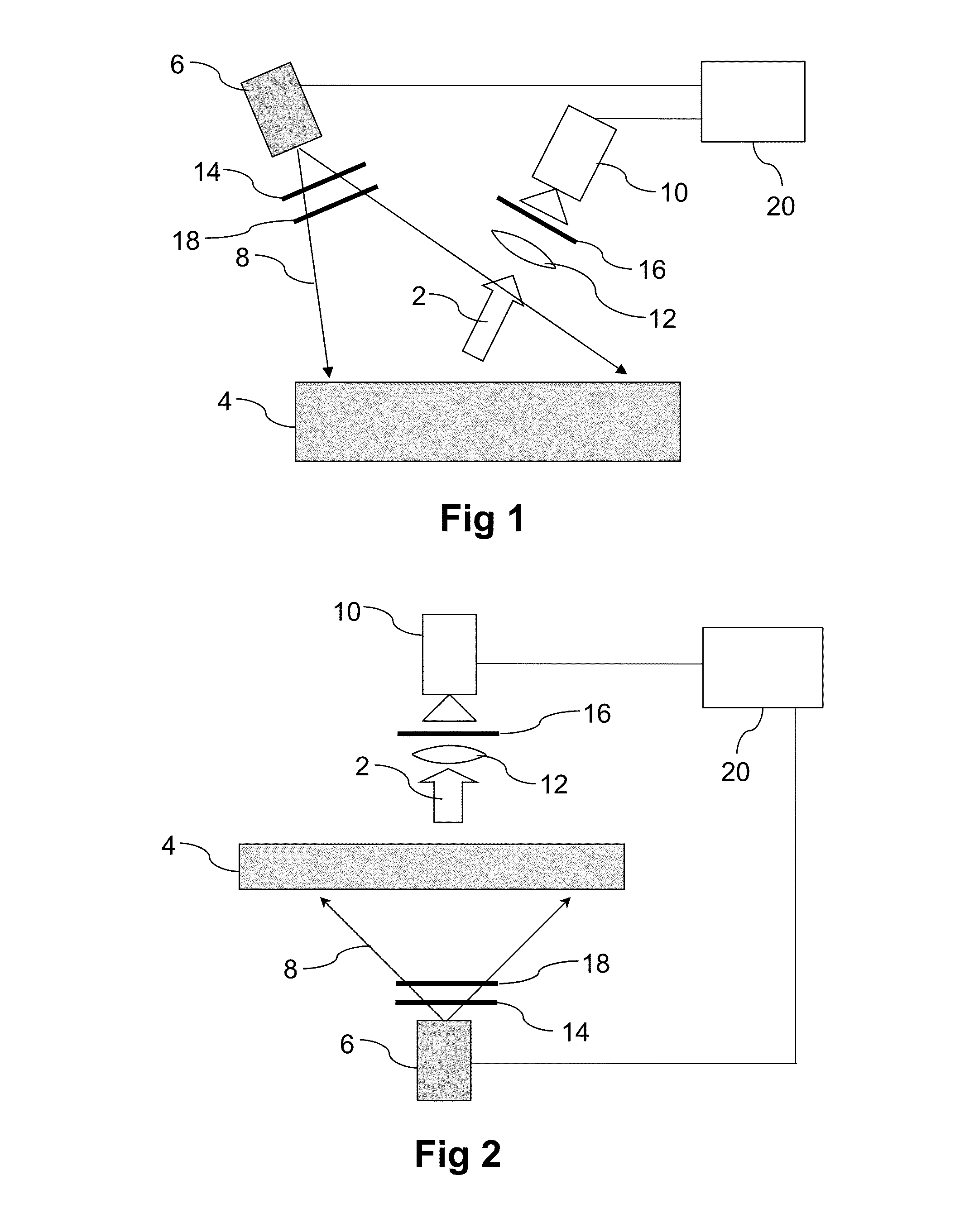
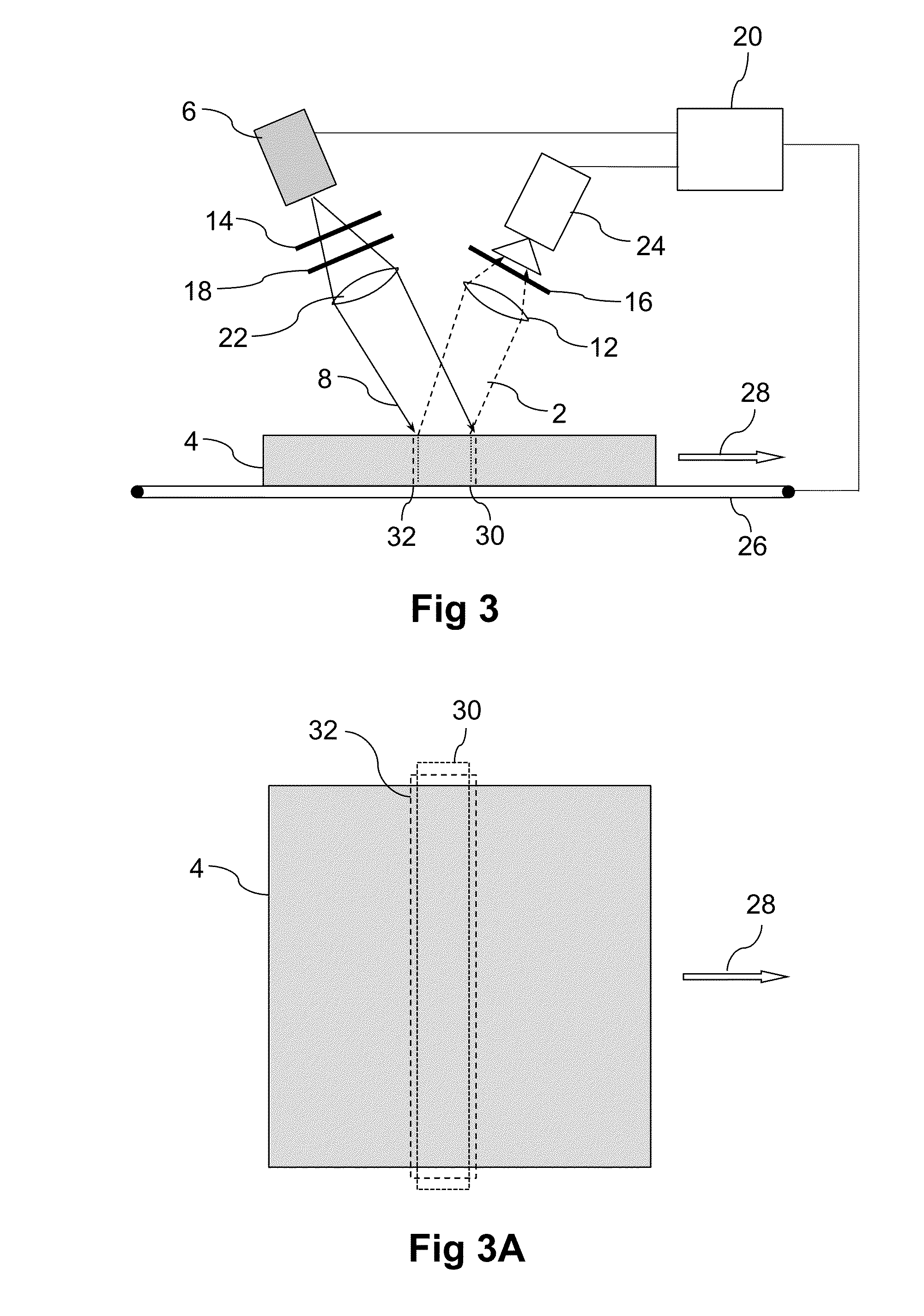
[0069]While FIG. 3 shows in schematic form a possible configuration of a line-scanning PL imaging system, a number of design aspects need to be considered to produce a system that can actually be used for routine in-line inspection of semiconductor samples such as silicon wafers on a photovoltaic cell line, whether at the incoming wafer stage (e.g. for sorting or grading purposes) or at one or more later stages in the cell manufacture process.
[0070]Firstly, it will be evident that line-scanning systems require the illuminated and imaged portions to be scanned across the sample, for example by moving the sample 4 relative to the light source 6 and image capture device 24. For small samples such as PV cells and wafers it is generally easiest to have the light source and image capture device stationary and move the sample on transport belts or rollers ...
PUM
 Abstract
Description
Claims
Application Information