Chip package structure

a technology of chip and package, applied in the direction of semiconductor devices, semiconductor/solid-state device details, electrical apparatus, etc., can solve the problems of inability to dispose of inductor, insufficient space for discharging inductor, and increasing the complexity of the chip packaging structure, so as to reduce the interference between the inducting coil and the chip, increase the area, and facilitate the effect of heat dissipation efficiency

Active Publication Date: 2015-06-18
CHIPMOS TECH INC
View PDF2 Cites 10 Cited by
  • Summary
  • Abstract
  • Description
  • Claims
  • Application Information

AI Technical Summary

Benefits of technology

[0007]The invention provides a chip package structure capable of increasing an area to design the inducting coil, reducing interference between an inducting coil and a chip, and facilitating a heat dissipating efficiency.
[0011]Based on the above, the inducting coil is disposed around the periphery region of the chip in the chip package structure of the invention to serve as an inductance element of the chip package structure. Thus, the area to dispose the inductance in the chip package structure is increased and no longer limited to the surface of the chip. The inductance of the chip package structure is consequently increased. Also, the inducting coil of the invention is disposed around the chip instead of being disposed on the active surface of the chip. Therefore, the signal interference between the inducting coil and the chip is reduced. Furthermore, in the chip package structure of the invention, the plurality of heat dissipating pillars may also be disposed around the periphery region of the chip, and the heat dissipating pillars are exposed by the molding compound. Consequently, the chip package structure is allowed to discharge heat generated by the chip through the heat dissipating pillars disposed around the chip, thereby facilitating the heat dissipating efficiency of the chip package structure and saving the cost of disposing an additional heat dissipating element such as a heat dissipating paste or heat sink, etc.

Problems solved by technology

With the advance of integration of integrated circuits, packaging structures of chips are more and more complicated and diversified.
Due to the trend to miniaturize the size of the chip, there is no enough space to dispose the inductor.
However, the heat dissipating sheet is not able to be firmly adhered to the package structure with such configuration, making the heat dissipating sheet ablated or detached from the package structure.
The yield rate and reliability in use of the products are thus influenced, not to mention that an additional cost for the heat dissipating sheets is required.

Method used


Image

  • Chip package structure
  • Chip package structure
  • Chip package structure

Examples


Embodiment Construction

[0021]It is to be understood that both the foregoing and other detailed descriptions, features, and advantages are intended to be described more comprehensively by providing embodiments accompanied with figures hereinafter. In the following embodiments, wordings used to indicate directions, such as “up,”“down,”“front,”“back,”“left,” and “right”, merely refer to directions in the accompanying drawings. Therefore, the directional wording is used to illustrate rather than limit the present invention. In addition, in the embodiments hereinafter, same or like elements are represented by same or like reference numerals.

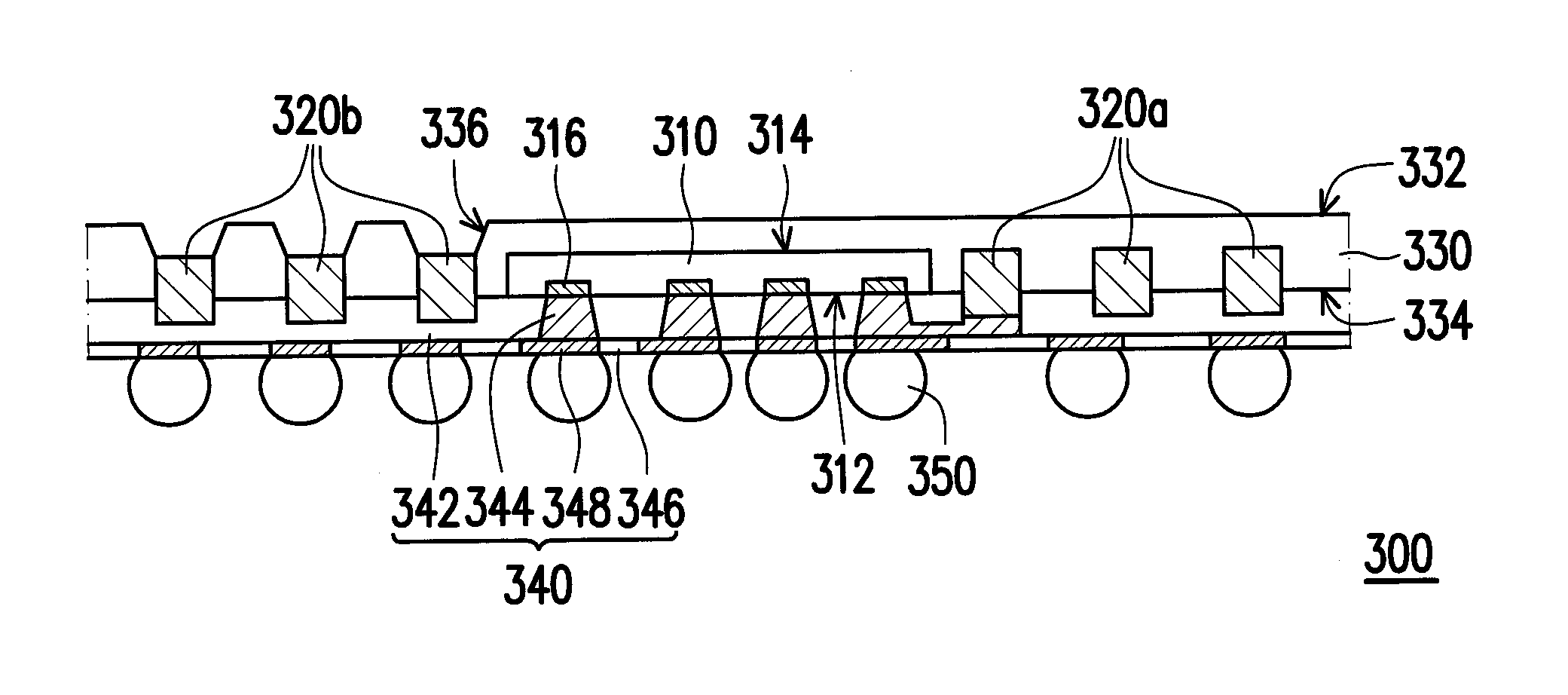
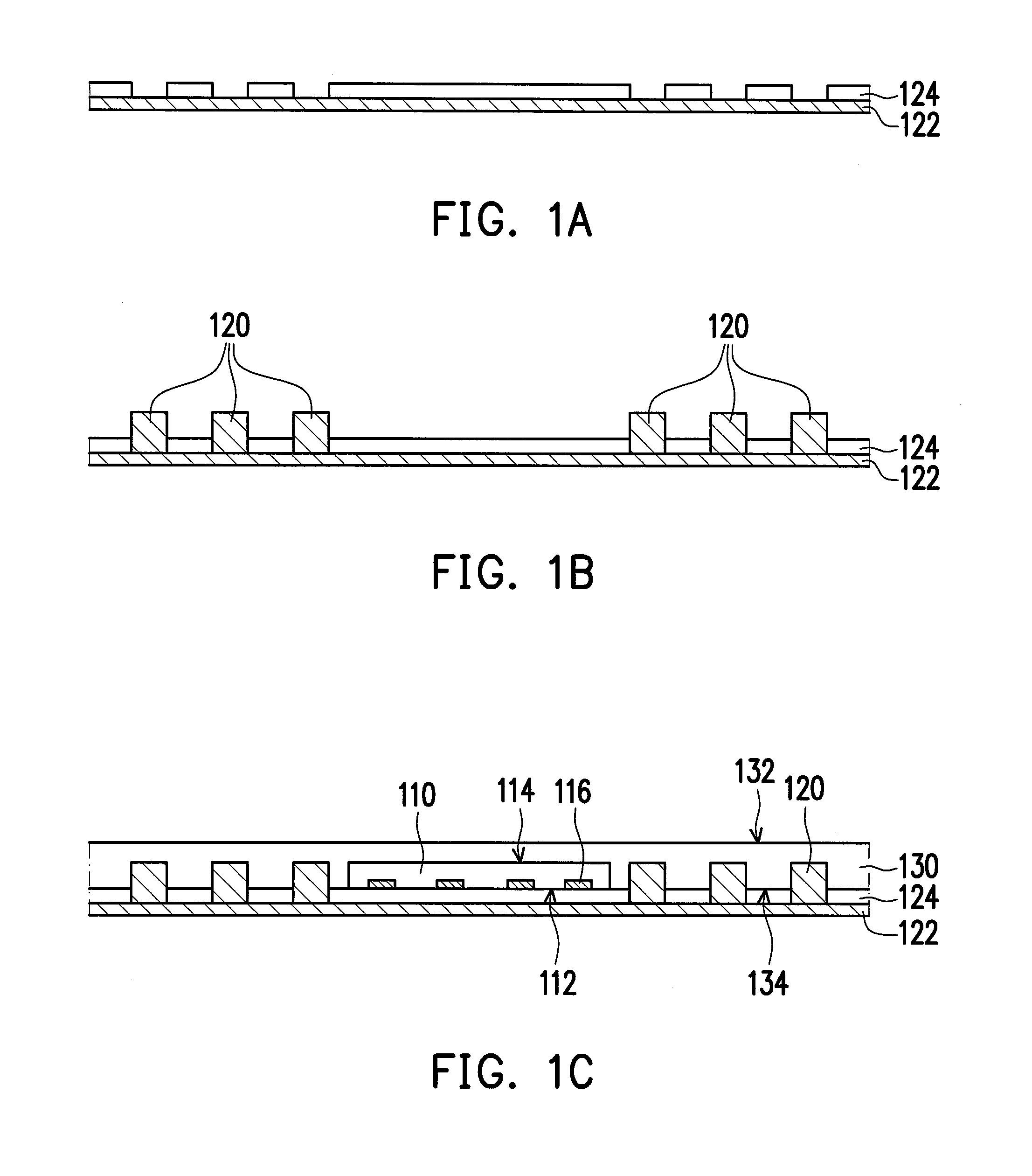
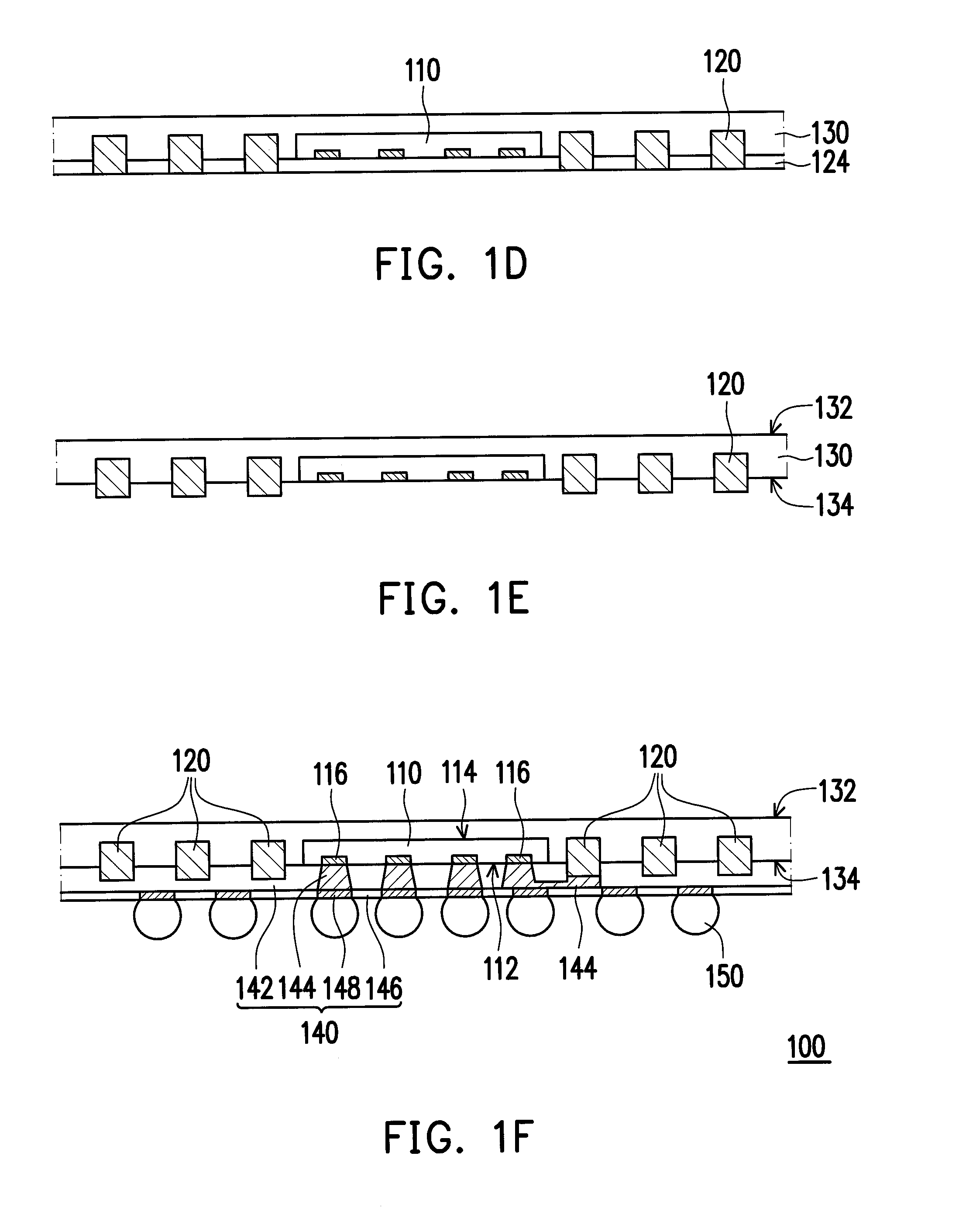
[0022]FIGS. 1A to 1F are schematic sectional views showing a flow of a manufacturing method of a chip package structure according to an embodiment of the invention. FIG. 2 is schematic bottom view of a configuration of an inducting coil and a chip according to an embodiment of the invention. FIG. 3 is schematic bottom view of a configuration of an inducting coil and a chip ...


PUM


Abstract

A chip package structure is provided. The chip package structure includes a chip, at least one inducting coil, a molding compound and a redistribution circuit layer. The chip includes an active surface, a back surface opposite to the active surface. The inducting coil is disposed around a periphery region of the chip. The molding compound covers the chip and the periphery region and exposes the active surface. The inducting coil is disposed at the molding compound. The redistribution circuit layer covers the active surface, part of the molding compound and part of the inducting coil, and electrically connects the chip.

Description

CROSS-REFERENCE TO RELATED APPLICATION[0001]This application claims the priority benefit of Taiwan application serial no. 102146307, filed on Dec. 16, 2013. The entirety of the above-mentioned patent application is hereby incorporated by reference herein and made a part of this specification.BACKGROUND OF THE INVENTION[0002]1. Field of the Invention[0003]The invention relates to a semiconductor package structure, and particularly relates to a chip package structure.[0004]2. Description of Related Art[0005]With the advance of integration of integrated circuits, packaging structures of chips are more and more complicated and diversified. Generally speaking, inductor is an essential passive device, which is widely used in radio frequency (RF) circuits, voltage controlled oscillators (VCO), low noise amplifiers (LNA) or other power amplifiers (PA).[0006]Usually, inductance is increased by increasing the number of turns of a coil in the manufacture of a high-frequency inductance element ...

Claims


Application Information

Patent Timeline
Patent Type & Authority Applications(United States)
IPC IPC(8): H01L23/522H01L23/367H01L23/31H01L23/528
CPCH01L23/5227H01L23/3114H01L23/367H01L23/528H01L23/4334H01L23/49816H01L23/49822H01L23/5389H01L2924/0002H01L23/3128H01L23/645H01L21/568H01L24/19H01L24/20H01L2224/04105H01L2924/19042H01L2224/12105H01L2224/18H01L23/3107H01L23/3677H01L23/5226H01L24/06H01L24/14H01L2224/0401H01L2224/05025H01L2224/13014H01L2224/13016H01L2924/00
Inventor LIAO, TSUNG-JEN
Owner CHIPMOS TECH INC
Why Eureka
Try Eureka