Accumulation-mode mosfet and driving method thereof

a technology of accumulation mode and mosfet, which is applied in the direction of oscillator, pulse technique, electronic switching, etc., can solve the problems of large consumption of such apparatus and unsuitability of apparatus for the recent energy saving trend

Active Publication Date: 2015-06-25
TOHOKU UNIV
View PDF4 Cites 5 Cited by
  • Summary
  • Abstract
  • Description
  • Claims
  • Application Information

AI Technical Summary

Problems solved by technology

The power consumption of such apparatus is large, and thus the apparatus is becoming unsuitable for the recent energy saving trend.
At the same time, it is an important issue to sufficiently improve the current driving capability upon power-on.

Method used


Image

  • Accumulation-mode mosfet and driving method thereof
  • Accumulation-mode mosfet and driving method thereof
  • Accumulation-mode mosfet and driving method thereof

Examples


Embodiment Construction

[0018]Some embodiments provide an accumulation-mode MOSFET in which the ratio between drain currents upon power-off (0 V) and power-on (power supply voltage) of the MOSFET is large and a current driving capability upon power-on is also large. Some embodiments provide an accumulation-mode MOSFET having high switching performance and a high current driving capability.

[0019]According to some embodiments, it is possible to provide an accumulation-mode MOSFET in which the ratio between drain currents upon power-off (0 V) and power-on (power supply voltage) is large and a current driving capability upon power-on is large, and a method of driving the accumulation-mode MOSFET. Furthermore, it is possible to provide an accumulation-mode MOSFET having high switching performance and a high current driving capability.

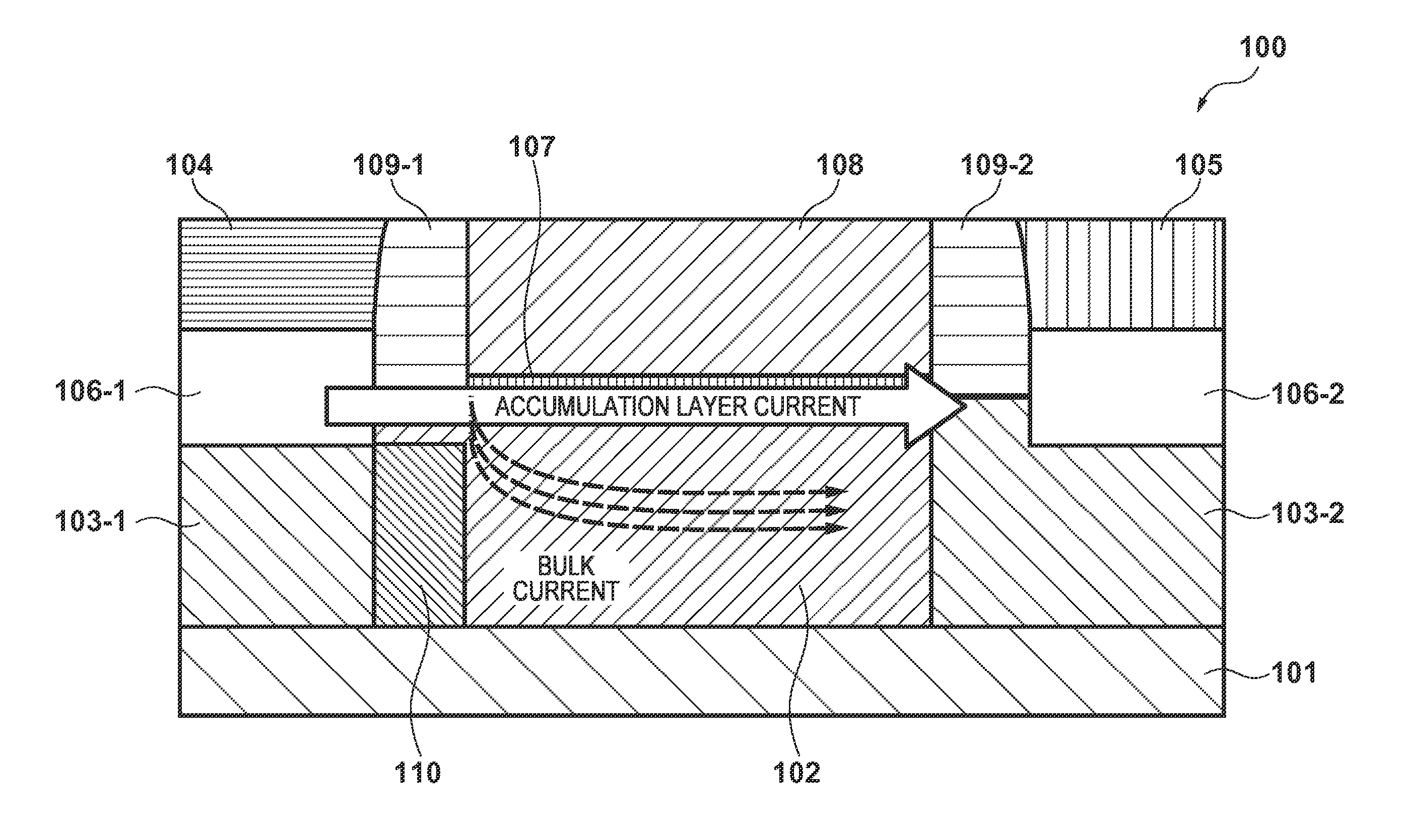
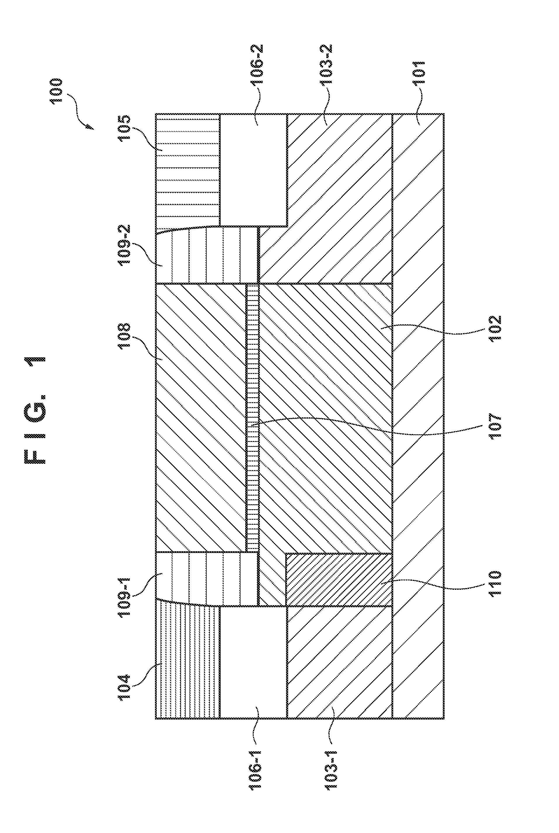
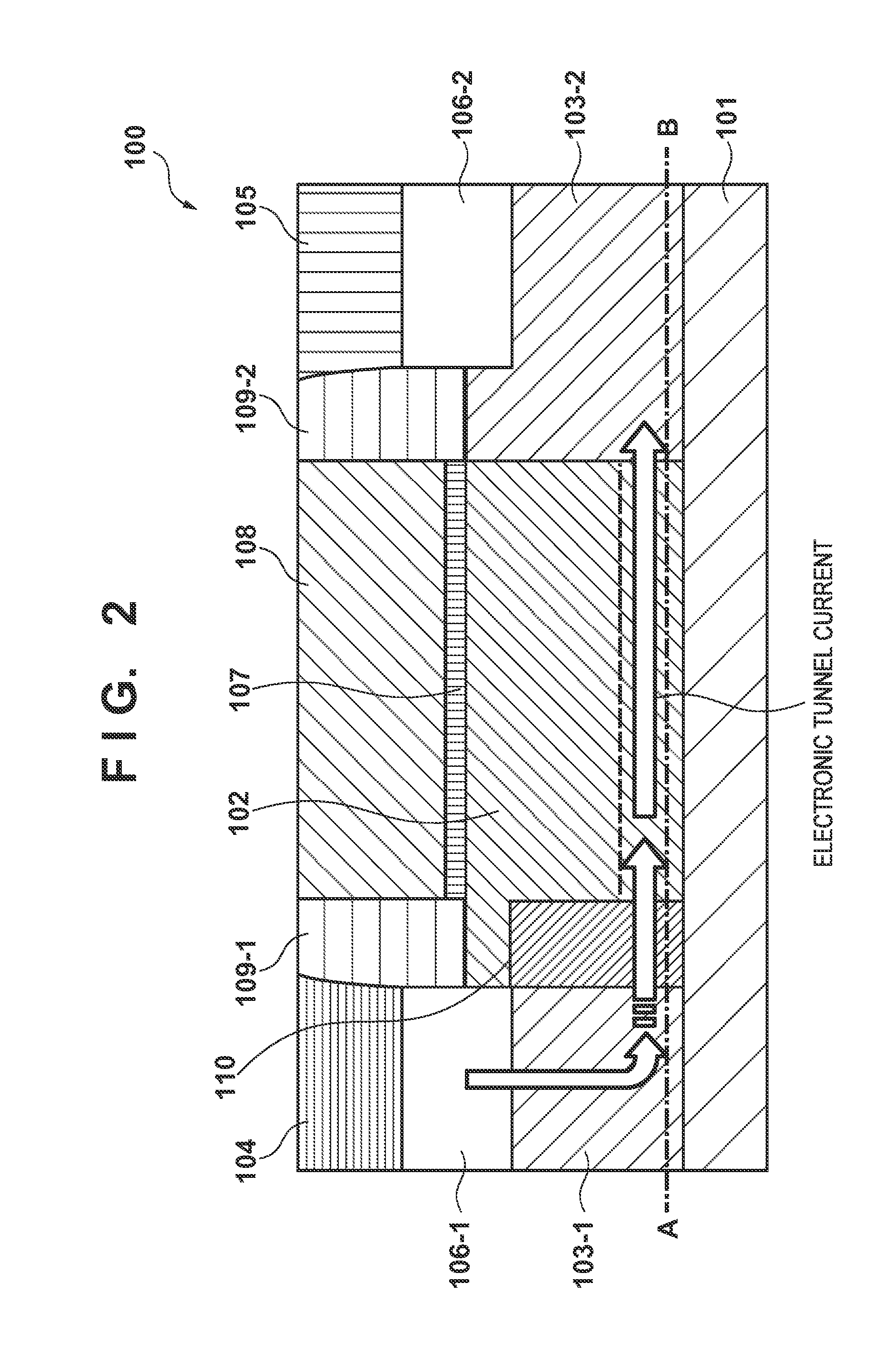
[0020]FIG. 1 is a schematic view for explaining the main parts of the structure of an accumulation-mode MOSFET according to a preferred embodiment of the present invention.

[0021]An...


PUM

PropertyMeasurementUnit
gate voltageaaaaaaaaaa
thicknessaaaaaaaaaa
equivalent oxide thicknessaaaaaaaaaa

Abstract

There is provided an accumulation-mode MOSFET. The accumulation-mode MOSFET has a tunnel electron emission portion and a thermionic emission portion which are provided in a source region portion.

Description

[0001]This application is a continuation of International Patent Application No. PCT / JP2012 / 006858 filed on Oct. 25, 2012, the entire content of which is incorporated herein by reference.BACKGROUND OF THE INVENTION[0002]1. Field of the Invention[0003]The present invention relates to an accumulation-mode MOSFET and a driving method thereof.[0004]2. Description of the Related Art[0005]In recent semiconductor integrated circuit apparatuses (to be also referred to as “LSI apparatuses” hereinafter), an enormous number (109 to 1012) of functional elements such as transistors are integrated at high density along with development of a micropatterning technique. The power consumption of such apparatus is large, and thus the apparatus is becoming unsuitable for the recent energy saving trend.[0006]To reduce the power consumption of the LSI apparatus, it is essential to decrease its power supply voltage. This is important not only in the semiconductor field but also in the semiconductor integr...

Claims


Application Information

Patent Timeline
Patent Type & Authority Applications(United States)
IPC IPC(8): H01L29/78H03K17/687H01L29/08
CPCH01L29/785H01L2029/7857H03K17/687H01L29/0895H01L29/7606H01L29/786
Inventor TERAMOTO, AKINOBU
Owner TOHOKU UNIV
Why Eureka
Try Eureka