

Silicon carbide semiconductor device and method for manufacturing same
a silicon carbide and semiconductor technology, applied in the field of silicon carbide semiconductor devices, can solve the problems of dielectric breakdown, easy overconcentration of electric field at the bottom, etc., and achieve the effect of preventing reducing overconcentration of electric field
- Summary
- Abstract
- Description
- Claims
- Application Information
AI Technical Summary
Benefits of technology
Problems solved by technology
Method used
Image

Examples
embodiment 1
Structure of Silicon Carbide Semiconductor Device
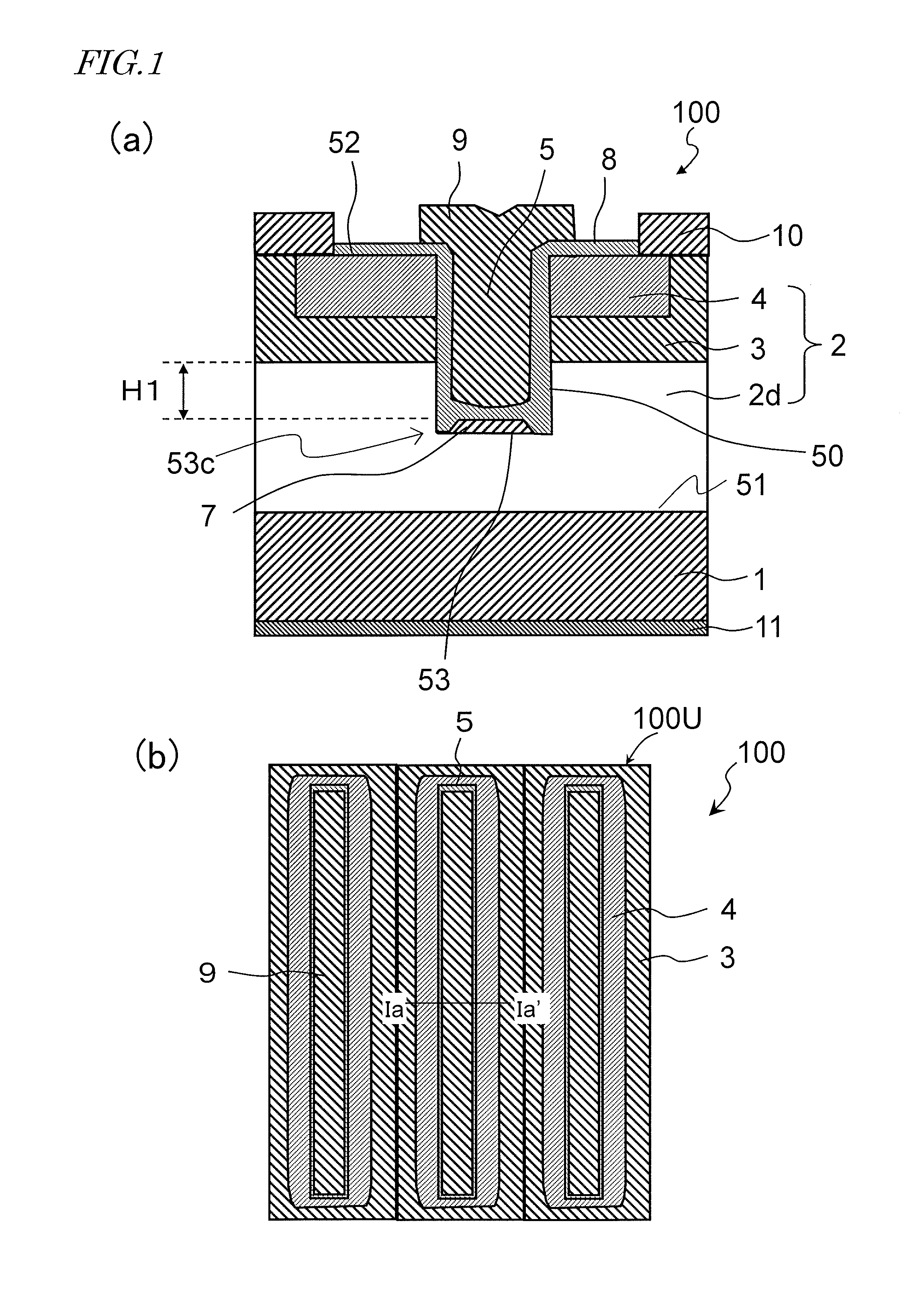
[0069]Hereinafter, an exemplary silicon carbide semiconductor device according to a first embodiment of the present disclosure will be described with reference to the accompanying drawings. In the following example, the silicon carbide semiconductor device is supposed to be a MISFET with a plurality of unit cells.
[0070]FIG. 1(a) schematically illustrates an exemplary cross-sectional structure of a single unit cell 100U in a silicon carbide semiconductor device according to this embodiment. FIG. 1(b) schematically illustrates an exemplary planar layout of a plurality of (e.g., three in this example) unit cells 100U on the surface of the silicon carbide layer 2 of the silicon carbide semiconductor device 100. FIG. 1(a) is a cross-sectional view as viewed on the plane Ia-Ia′ shown in FIG. 1(b). FIG. 1(b) illustrates the arrangement of a body region 3, a source region 4, gate electrodes 9 and trenches 5 with illustration of some other mem...
embodiment 2
Structure of Silicon Carbide Semiconductor Device
[0130]Next, an exemplary silicon carbide semiconductor device according to a second embodiment of the present disclosure will be described with reference to the accompanying drawings.
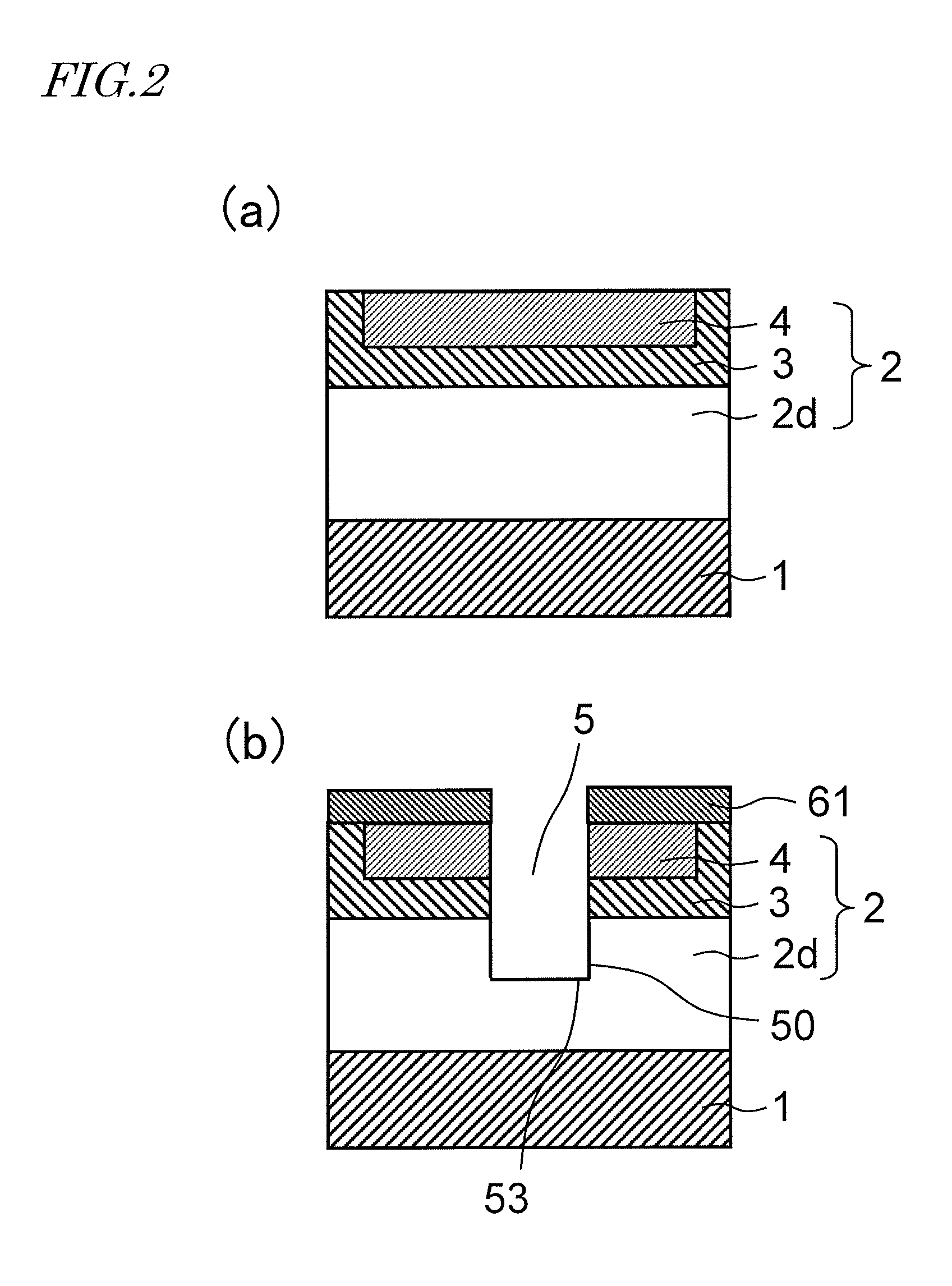
[0131]FIG. 7 is a cross-sectional view schematically illustrating an exemplary cross-sectional structure of a single unit cell in a silicon carbide semiconductor device 200 according to this embodiment. In the silicon carbide semiconductor device 200 of this embodiment, its trench bottom impurity layer 7 has a different shape from its counterpart of the silicon carbide semiconductor device 100 of the first embodiment. In FIG. 7, any component also included in the silicon carbide semiconductor device 100 shown in FIG. 1 and having substantially the same function as its counterpart is identified by the same reference numeral as its counterpart's and description thereof will be omitted herein.
[0132]As shown in FIG. 7, in this silicon carbide semiconductor de...
embodiment 3
Structure of Silicon Carbide Semiconductor Device
[0168]Next, an exemplary silicon carbide semiconductor device according to a third embodiment of the present disclosure will be described with reference to the accompanying drawings.
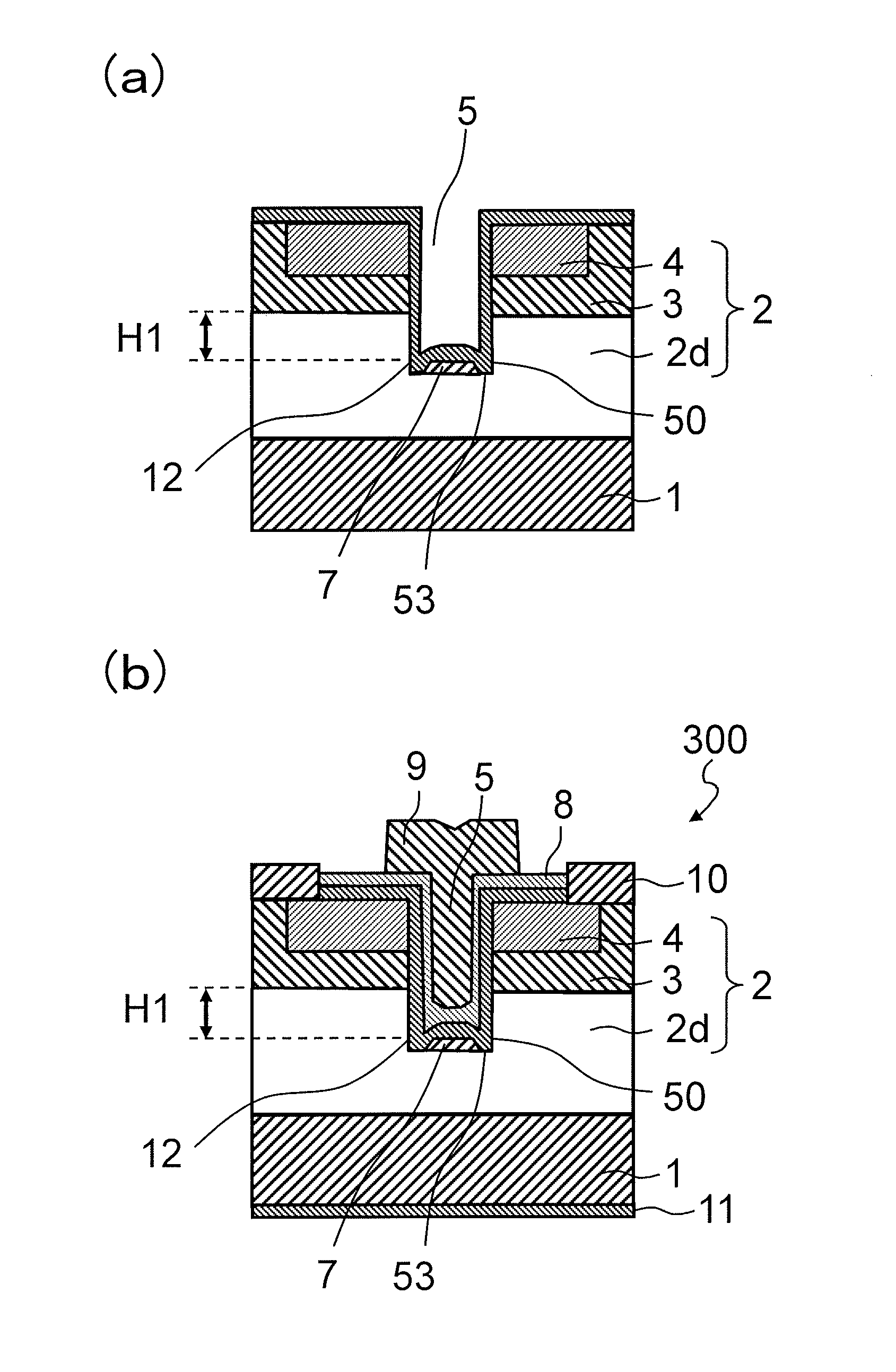
[0169]FIG. 13 is a cross-sectional view schematically illustrating an exemplary cross-sectional structure of a single unit cell in a silicon carbide semiconductor device 300 according to this embodiment. The silicon carbide semiconductor device 300 of this embodiment includes a channel layer 12 of the first conductivity type, which is a difference from the silicon carbide semiconductor device 100 of the first embodiment. In FIG. 13, any component also included in the silicon carbide semiconductor device 100 shown in FIG. 1 and having substantially the same function as its counterpart is identified by the same reference numeral as its counterpart's and description thereof will be omitted herein.
[0170]As shown in FIG. 13, the silicon carbide semiconductor de...
PUM
| Property | Measurement | Unit |
|---|---|---|
| temperature | aaaaa | aaaaa |
| breakdown voltage | aaaaa | aaaaa |
| angle | aaaaa | aaaaa |
Abstract
Description
Claims
Application Information