
Semiconductor component with chip for the high-frequency range

Active Publication Date: 2015-06-25
SHARP KK +1
View PDF7 Cites 1 Cited by
  • Summary
  • Abstract
  • Description
  • Claims
  • Application Information

AI Technical Summary

Benefits of technology

This patent describes a new design for components that are used in electronic devices. These components have improved heat removal, better control, and easier manufacturing. The components are designed to have elastic connecting tabs that compensate for thermal expansion and reduce mechanical stresses, which can prolong the lives of the components. The components can be easily fitted onto printed-circuit boards, allowing for cost-effective and reliable assembly. Additionally, the components can have a reduced heat capacity, which makes it easier to achieve a reliable soldering process. Overall, this design can improve the performance and reduce the cost of components used in electronic devices.

Problems solved by technology

For example, high-frequency switching circuits can provide considerable thermal-power losses during operation.
With the known packaging solutions, an adequate heat removal is not possible without difficulty.
Additionally or alternatively, resonators may be required for high-frequency components or respectively switching circuits, which, in the case of the known packaging solutions, cannot be provided in the required manner and / or in a cost-favourable manner.
However, the lack of SMD capability counteracts this improved heat removal.

Method used


Image

  • Semiconductor component with chip for the high-frequency range
  • Semiconductor component with chip for the high-frequency range
  • Semiconductor component with chip for the high-frequency range

Examples


Embodiment Construction

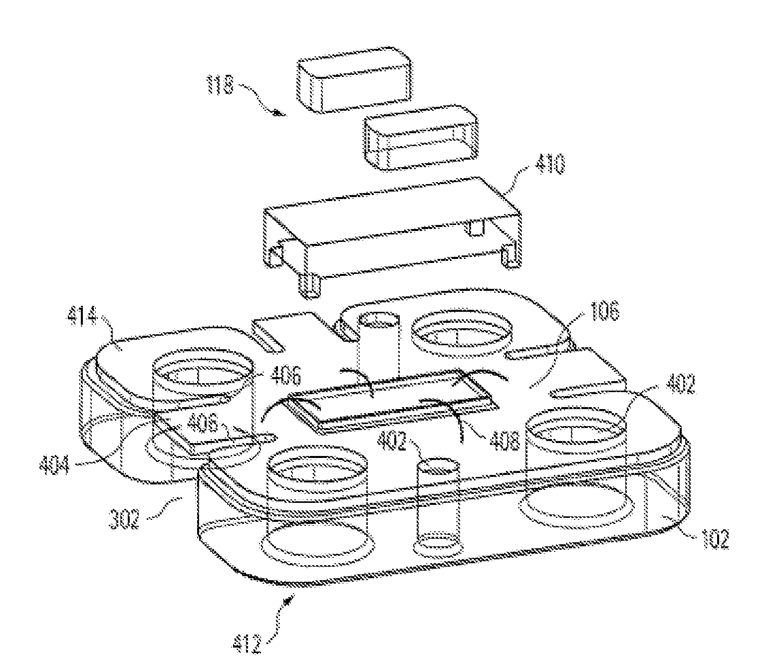
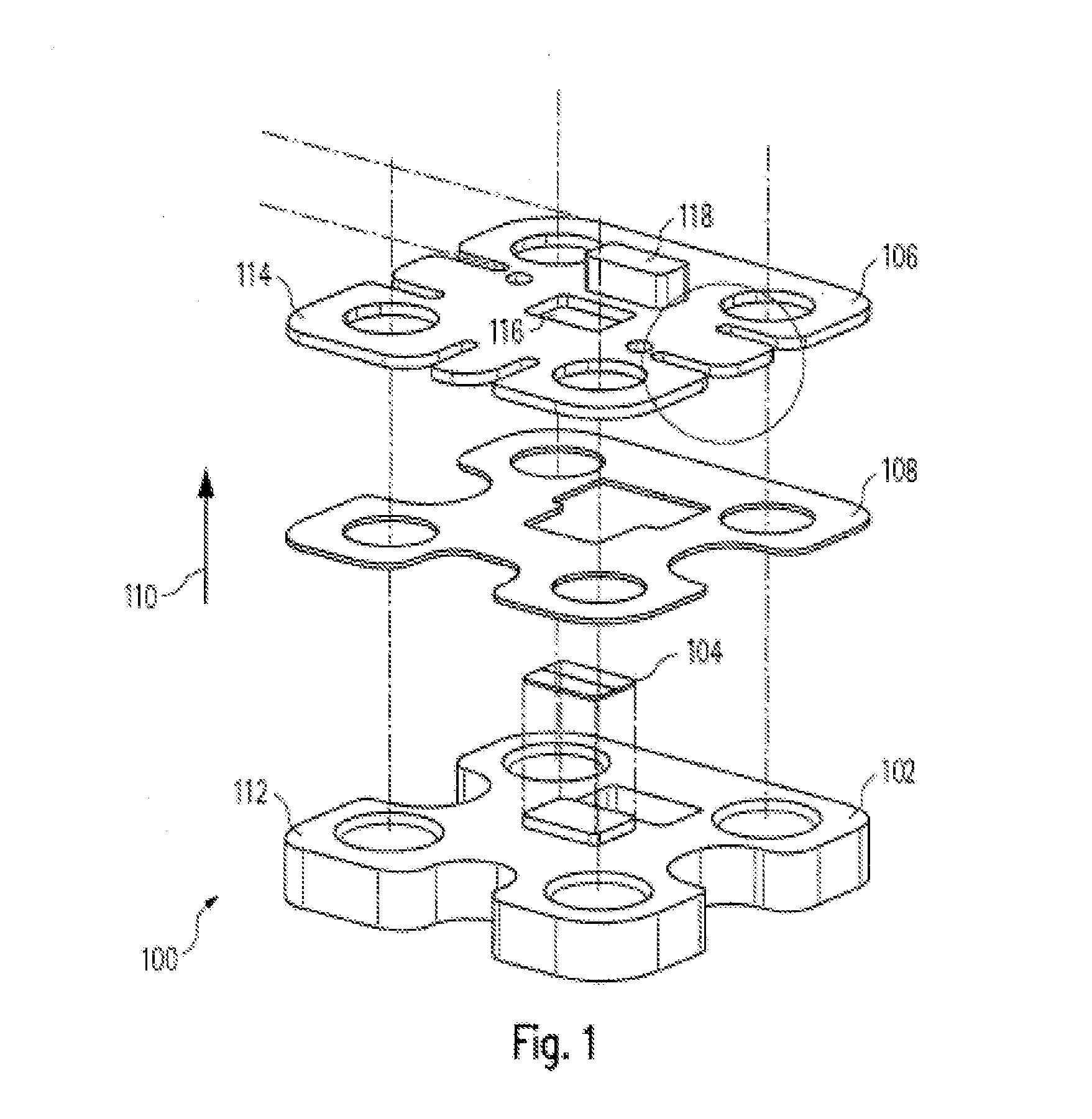
[0076]In the form of an exploded diagram, FIG. 1 visualises the construction of a semiconductor component 100 according to an exemplary embodiment of the invention. The component 100 comprises a metal body 102, a chip 104 and a supplementary circuit board 106 which is attached by means of a bond layer 108 to the metal body 102.

[0077]For purposes of explanation, it is assumed that the chip 104 is an active chip with high thermal output during operation. Further chips or components with comparatively insubstantial thermal output can be additionally present and will not be discussed in further detail. The chip 104 can implement, for example, a high-frequency application and, in particular, can be an MMIC. With other exemplary embodiments, several chips can also be provided on a metal body and or a supplementary circuit board or several supplementary circuit boards.

[0078]In the assembled condition, the component 100 is provided in the form of a package, for example, an ASIC package, for...


PUM

PropertyMeasurementUnit
Distanceaaaaaaaaaa
Frequencyaaaaaaaaaa
Semiconductor propertiesaaaaaaaaaa

Abstract

The invention relates to a semiconductor component with a chip, especially with a high-frequency switching circuit. The semiconductor component further comprises a metal body on the chip and a supplementary circuit board. The supplementary circuit board is provided on an underside facing away from the metal body for connection with a printed-circuit board by means of reflow soldering.

Description

RELATED APPLICATION[0001]This application claims priority to German Patent Application No. 10 2013 226 989.7 filed on Dec. 20, 2013, which is hereby incorporated by reference.FIELD[0002]The present invention relates to a semiconductor component with a chip, especially with a high-frequency switching circuit, and a printed-circuit board fitted with the component, a method for the manufacture of the component and a method for fitting a printed-circuit board with the component.BACKGROUND[0003]In high-frequency switching circuits, typical control or signal frequencies are disposed approximately within the microwave range, that is, between 300 MHz (megahertz) and 300 GHz. Such switching circuits are used in different fields, for example, in power amplification, low-noise amplification, for high-frequency switches and so on. Switching circuits can be embodied as integrated circuits, that is, for example, in the form of one or more chips. ICs of this kind can be embodied, for example, as M...

Claims


Application Information

Patent Timeline
IPC IPC(8): H05K1/18H01L23/04B23K1/00H05K1/02H05K3/34H01L23/00H05K1/14
CPCH05K1/182H05K2203/043H01L24/86H01L24/50H01L24/48H01L23/04H05K1/141H05K1/0237H05K3/341H05K3/3478B23K1/0016H01L2224/86815H01L2224/85815H01L2224/48091H01L2224/48227H01L24/85B23K1/008H01L2924/181H01L2924/00014H01L23/043H05K1/021H05K1/0243H05K1/117H05K1/144H05K2201/041H05K2201/09063H05K2201/09618H05K2201/10409H01L2224/291H01L2224/32245H01L2224/48157B23K2101/42H01L2924/00H01L2224/45099H01L2224/05599H01L2924/014
Inventor HAGENEDER, DANIELKAPPELS, MARTIN
Owner SHARP KK
Learn More