Mounting structure and method for supplying reinforcing resin material

a technology of reinforcing resin and mounting structure, which is applied in the direction of manufacturing tools, electrical apparatus construction details, and non-printed electrical components of printed circuits. it can solve the problems of increasing manufacturing cost and manufacturing steps, increasing manufacturing costs and manufacturing steps, and needing to form holes for fixing the tying band on the substrate. , to achieve the effect of minimizing design restrictions, high reliability and easy supply

Active Publication Date: 2015-06-25
PANASONIC INTELLECTUAL PROPERTY MANAGEMENT CO LTD
View PDF4 Cites 1 Cited by
  • Summary
  • Abstract
  • Description
  • Claims
  • Application Information

AI Technical Summary

Benefits of technology

[0029]According to the present invention, the reinforcing resin body bonded to the substrate and the electronic component includes the multiple reinforcing resin layers that are stacked in the height direction of the raised electronic component so as to be raised from the substrate along the side of the electronic component. Thus, even if the electronic component to be reinforced is a large electronic component that is thick in profile and receives large vibrations and so on, for example, a stress caused by vibrations is spread and absorbed in the contact portion of the reinforcing resin layers, thereby satisfactorily keeping the reinforcing function. Hence, the mounting structure can have high reliability. The reinforcing body includes a resin body that is provided along the side of the electronic component so as to be raised from the substrate, and thus the reinforcing body can be easily supplied according to the size of the electronic component. Moreover, this configuration eliminates the need for forming holes or the like on the substrate, thereby minimizing design restrictions.
[0030]The reinforcing resin layers of the reinforcing resin body are stacked in the height direction of the electronic component, the reinforcing resin layer having one end that is extended in the width direction of the side of the electronic component and then is folded toward the opposite side in the width direction so as to continue to one end of another reinforcing resin layer adjacent to the reinforcing resin layer in the height direction of the electronic component. With this configuration, the reinforcing resin layers vertically adjacent to each other are stacked on top of each other in the vertical direction with the ends folded in a continuous manner. Hence, the connecting portion of the ends of the reinforcing resin layers also elastically absorbs a stress caused by vibrations, thereby further improving the stress absorbing function. This can more satisfactorily keep the reinforcing function, allowing the mounting structure to have higher reliability.
[0031]Furthermore, the reinforcing resin layers of the reinforcing resin body decrease in dimension in the width direction of the side of the electronic component as the height from the substrate increases or the reinforcing resin layers decrease in thickness along the side of the electronic component as the height from the substrate increases. This configuration can satisfactorily reinforce the electronic component in a relatively stable state with the reinforcing resin body having a small volume, thereby reducing the manufacturing cost and the weight of the mounting structure.
[0032]Moreover, the reinforcing resin body covers at least a part of the top surface of the electronic component. With this configuration, the reinforcing resin body covers the top surface of the electronic component as well as the side of the electronic component, thereby increasing the reinforcing force of the reinforcing resin body. This configuration can also improve the reliability of the mounting structure.
[0033]According to the method for supplying a reinforcing resin material, the reinforcing resin material is supplied widely in the width direction of the side of the electronic component along the side of the electronic component so as to form the at least one reinforcing resin layer, and the following process is repeated: the reinforcing resin material at the end position of the at least one reinforcing resin layer is continuously supplied and is moved in the height direction of the electronic component so as to separate from the substrate, and then the reinforcing resin material is folded toward the opposite side in the width direction, the at least one reinforcing resin layer including multiple reinforcing resin layers stacked in the height direction of the electronic component. This method can form the reinforcing resin body with high working efficiency and thus reduce the manufacturing process and the manufacturing time of the mounting structure, thereby suppressing the manufacturing cost of the mounting structure.
[0034]Moreover, according to the method for supplying a reinforcing resin material, the resin supply unit that supplies the reinforcing resin material includes the supply nozzle. The supply nozzle is disposed near the side of the electronic component, in an upright position relative to the mounting surface of the substrate where the electronic component is mounted, and the supply nozzle is moved along the side of the electronic component while the reinforcing resin material is supplied so as to circumferentially extend larger than the diameter of the supply nozzle. This configuration can easily control the posture of the supply nozzle. Moreover, even in the case of a small gap around the electronic component, the reinforcing resin material can be satisfactorily supplied. The mounting structure can be satisfactorily applied to most electronic components.

Problems solved by technology

However, if a large external force is likely to be applied to an electronic component, only a solder joint on the electronic component may not have sufficient bonding strength.
In this structure, however, the reinforcing component 61 needs to be fabricated again according to a size change of the electronic component 60, increasing the manufacturing cost and the number of manufacturing steps.
In this case, however, the hole for fixing the tying band needs to be formed on the substrate.
This further limits the design with restricted applicability.
However, this method may increase the manufacturing cost and the number of manufacturing steps, further limiting the design with restricted applicability.
As has been discussed, the conventional mounting structure and method for an electronic component cannot simultaneously achieve the function of obtaining a sufficient reinforcing effect for a relatively large electronic component and the function of easily responding to a change of the shape of the electronic component.

Method used


Image

  • Mounting structure and method for supplying reinforcing resin material
  • Mounting structure and method for supplying reinforcing resin material
  • Mounting structure and method for supplying reinforcing resin material

Examples


eleventh and twelfth embodiments

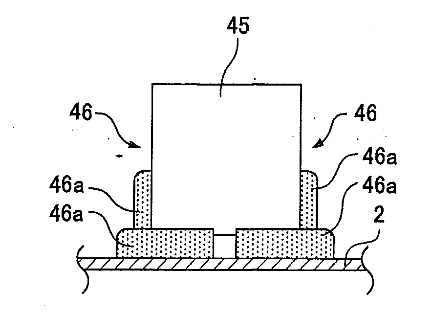
[0144]FIGS. 12A to 12C and 13A to 13C show a rectangular electronic component 9. As shown in FIGS. 12A to 12C, two reinforcing resin bodies 37 and reinforcing resin layers 37a constituting the reinforcing resin bodies 37 may be formed over one sides 9g as well as corners 9f of the electronic component 9. As shown in FIGS. 13A to 13C, four reinforcing resin bodies 38 and reinforcing resin layers 38a constituting the reinforcing resin bodies 38 may be formed only over corners 9f of the electronic component 9.

[0145]In FIGS. 12A to 12C and 13A to 13C, reference numeral 9a denotes the side of the electronic component 9, reference numeral 9b denotes the top surface of the electronic component 9, and reference numeral 9d denotes the connecting terminals of the electronic component 9. Moreover, in FIGS. 12A to 12C and 13A to 13C, one ends of the reinforcing resin layers 37a and 38a of the reinforcing resin bodies 37 and 38 are extended in the width direction of the side 9a of the electronic...


PUM

PropertyMeasurementUnit
heightaaaaaaaaaa
widthaaaaaaaaaa
volumeaaaaaaaaaa

Abstract

A mounting structure for an electronic component and a method for mounting the electronic component are provided with a sufficient reinforcing effect for the relatively tall electronic component raised from a substrate. The mounting structure and the mounting method can easily respond to a change of the shape of the electronic component. In a mounting structure 1, a substrate 2 and an electronic component 4 raised on the substrate 2 are joined with bonding metal 3 and a reinforcing resin body 5 is bonded to the substrate 2 and the electronic component 4. The reinforcing resin body 5 includes a plurality of reinforcing resin layers 5a. The reinforcing resin layers 5a constituting the reinforcing resin body 5 are stacked in the height direction of the raised electronic component 4 along a side 4a of the electronic component 4 so as to be raised from the substrate 2.

Description

FIELD OF THE INVENTION[0001]The present invention relates to a mounting structure including an electronic component mounted on a substrate, and a method for supplying a reinforcing resin material disposed in the mounting structure.BACKGROUND OF THE INVENTION[0002]Conventionally, electronic components have been joined and mounted onto a substrate, e.g., a printed circuit board with bonding metal such as solder in widespread application. However, if a large external force is likely to be applied to an electronic component, only a solder joint on the electronic component may not have sufficient bonding strength.[0003]As shown in FIGS. 28 and 29, a solution to this problem is to apply reinforcing resin 54 along the side of an electronic component 52 that is not only bonded to a substrate 53 with solder (solder balls in FIG. 28) 51, but also allows the reinforcing resin 54 to bond the electronic component 52 onto the substrate 53 with reinforced holding power at a joint (for example, Jap...

Claims


Application Information

Patent Timeline
Patent Type & Authority Applications(United States)
IPC IPC(8): H05K7/02H05K13/04
CPCH05K13/04H05K7/02H05K3/301H05K2201/10583H05K3/284H05K3/3447H05K2201/10159H05K2201/10674H05K1/182H05K2201/10007H05K1/181H05K1/162H05K1/165H05K1/167
Inventor TOKII, SEIJITASAKI, MANABU
Owner PANASONIC INTELLECTUAL PROPERTY MANAGEMENT CO LTD
Why Eureka
Try Eureka