Laminated substrate, light-emitting device, and method for producing light-emitting device

a technology of light-emitting devices and laminated substrates, which is applied in the direction of sustainable manufacturing/processing, final product manufacturing, transportation and packaging, etc., can solve the problems of low mechanical strength, high cost, and high cost, and achieve satisfactory visibility

Active Publication Date: 2015-07-16
SAMSUNG DISPLAY CO LTD
View PDF4 Cites 18 Cited by
  • Summary
  • Abstract
  • Description
  • Claims
  • Application Information

AI Technical Summary

Benefits of technology

[0013]One disclosed embodiment of the present disclosure provides a light-emitting device configured to suppress reflection to provide satisfactory visibility.

Problems solved by technology

Thus, the second method has problems with the accuracy of dimensions in pattern processing and the accuracy of registration of patterns.
Thus, the electronic device element is likely to break at the time of transfer because of its low mechanical strength.
The plastic film and the supporting glass substrate are less likely to be easily separated from each other because of high adhesion between the plastic film and the supporting glass substrate.

Method used


Image

  • Laminated substrate, light-emitting device, and method for producing light-emitting device
  • Laminated substrate, light-emitting device, and method for producing light-emitting device
  • Laminated substrate, light-emitting device, and method for producing light-emitting device

Examples


first embodiment

1. Structure of Display Device

[0104]The structure of a display device according to a first embodiment of the present disclosure will be described below with reference to FIGS. 1 and 2 by taking, as an example, an active-matrix organic EL display device for which the structure is used.

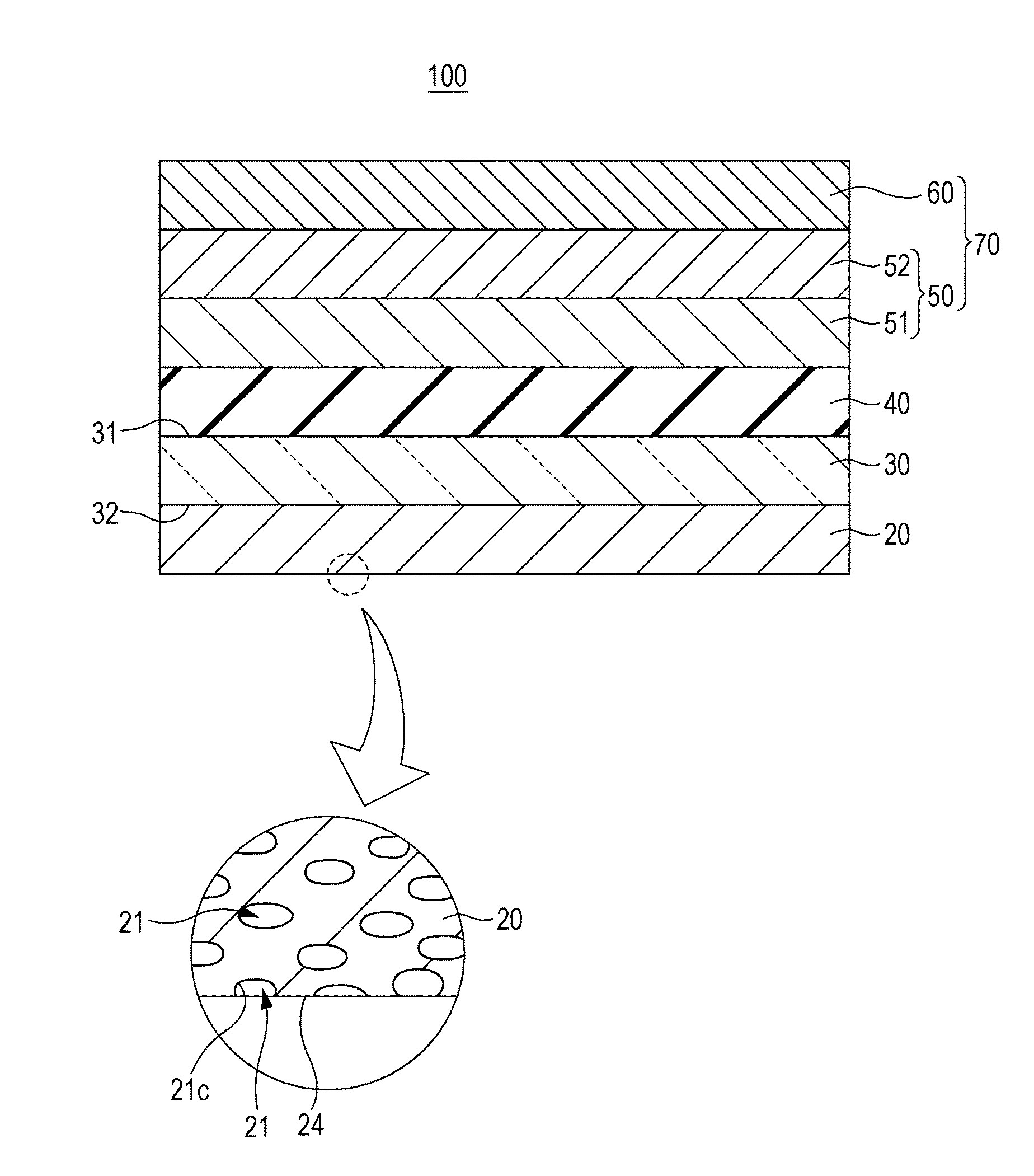
[0105]FIG. 1 is a schematic, partial cross-sectional view of the structure of a display device 100 according to this embodiment. In this embodiment, the display device 100 is an active-matrix organic EL display device.

[0106]As illustrated in FIG. 1, the display device 100 includes a porous layer 20, a transparent substrate 30, a sealing layer 40, a TFT layer 50, and an organic EL element layer 60 stacked in that order. The TFT layer 50 includes an electrode layer 51 and a TFT main body layer 52. The TFT layer 50 and the organic EL element layer 60 constitute a display device element layer (or a display device element) 70. The display device 100 includes the display device element layer 70 above an upper...

third modification

[0181]In the second modification, the second resin material for the formation of the second porous sublayer 220b desirably has a higher viscosity than that of the first resin material for the formation of the first porous sublayer 220a. In this case, the second resin material for the formation of the second porous sublayer 220b is less likely to enter the pores in the first porous sublayer 220a, thereby maintaining the porosity of the first porous sublayer 220a.

Fourth Modification

[0182]In the second modification, the case where the average diameter of the pores in the first porous sublayer 220a is smaller than the average diameter of the pores in the second porous sublayer 220b has been described. However, the present disclosure is not limited thereto. The average diameter of the pores in the first porous sublayer 220a may be larger than the average diameter of the pores in the second porous sublayer 220b.

[0183]In this case, the effect of scattering light is enhanced in the first ...

eighth modification

[0187]In the case where the transparent substrate 30 is formed by the application of a resin material, affinity treatment may be performed after a step of forming the porous layer 20 and before a step of forming the transparent substrate 30. The affinity treatment may be performed such that the affinity of a surface 23 of the porous layer 20 (i.e. a main surface of the porous layer 20 on the side on which the transparent substrate 30 is to be formed) for the resin material used to form the transparent substrate 30 (hereinafter, referred to simply as “resin affinity”) is higher than the resin affinity of the inner surfaces 21c of the pores 21 exposed at the surface 23.

[0188]A method of the affinity treatment will be described below with reference to FIGS. 10A to 11C.

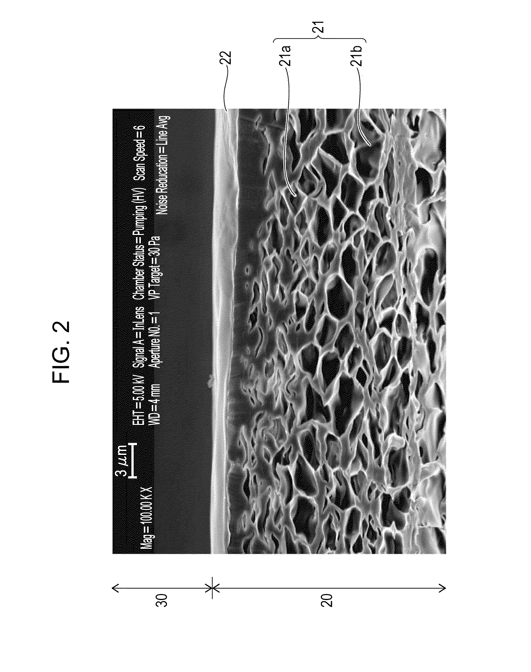
[0189]FIG. 10A is a partial cross-sectional view illustrating a state in which the porous layer 20 is formed on the supporting substrate 10. As illustrated in the figure, the inner surfaces 21c of some pores 21 are expose...


PUM

PropertyMeasurementUnit
diameteraaaaaaaaaa
diameteraaaaaaaaaa
diameteraaaaaaaaaa

Abstract

A light-emitting device includes a transparent substrate, a light-emitting element arranged on or above one main surface of the transparent substrate, and a porous layer arranged on or above the other main surface of the transparent substrate, the porous layer being an organic material layer having a plurality of pores. Inner surfaces of some pores among the plurality of pores may be exposed at a main surface of the porous layer opposite to a side on which the transparent substrate lies. A gas may be present in the pores the inner surfaces of which are exposed.

Description

[0001]This application claims priority to Japanese Patent Application Nos. 2014-004451 and 2014-004452, filed on Jan. 14, 2014, the contents of which are hereby incorporated by reference.BACKGROUND[0002]1. Technical Field[0003]The present disclosure relates to a laminated substrate, a light-emitting device, and a method for producing a light-emitting device.[0004]2. Description of the Related Art[0005]In general, display devices, such as liquid crystal displays (LCDs) and organic electroluminescence (EL) displays, have structures in which various layers, such as an electrode layer formed of a metal thin film, a thin film transistor (TFT) layer, an insulating layer, a light-emitting layer, a sealing layer configured to prevent the penetration of water or oxygen from the outside, a color filter, a polarizer, and a protective layer configured to prevent damage due to mechanical stress from the outside, are stacked on a substrate, for example, a glass substrate or a plastic substrate (f...

Claims


Application Information

Patent Timeline
Patent Type & Authority Applications(United States)
IPC IPC(8): H01L33/20
CPCH01L2933/0008H01L33/20H01L27/1266H01L21/6835H01L2221/6835H01L2221/68381Y02E10/549Y10T428/249991Y02P70/50H10K71/80H10K77/111H10K50/844H10K50/854
Inventor OKUMOTO, KENJITANAKA, YUJI
Owner SAMSUNG DISPLAY CO LTD
Why Eureka
Try Eureka