Eureka AIR delivers breakthrough ideas for toughest innovation challenges, trusted by R&D personnel around the world.

Circuit connecting adhesive film and circuit connecting structure

Inactive Publication Date: 2010-09-02
HITACHI CHEM CO LTD
View PDF4 Cites 8 Cited by
  • Summary
  • Abstract
  • Description
  • Claims
  • Application Information

AI Technical Summary

Benefits of technology

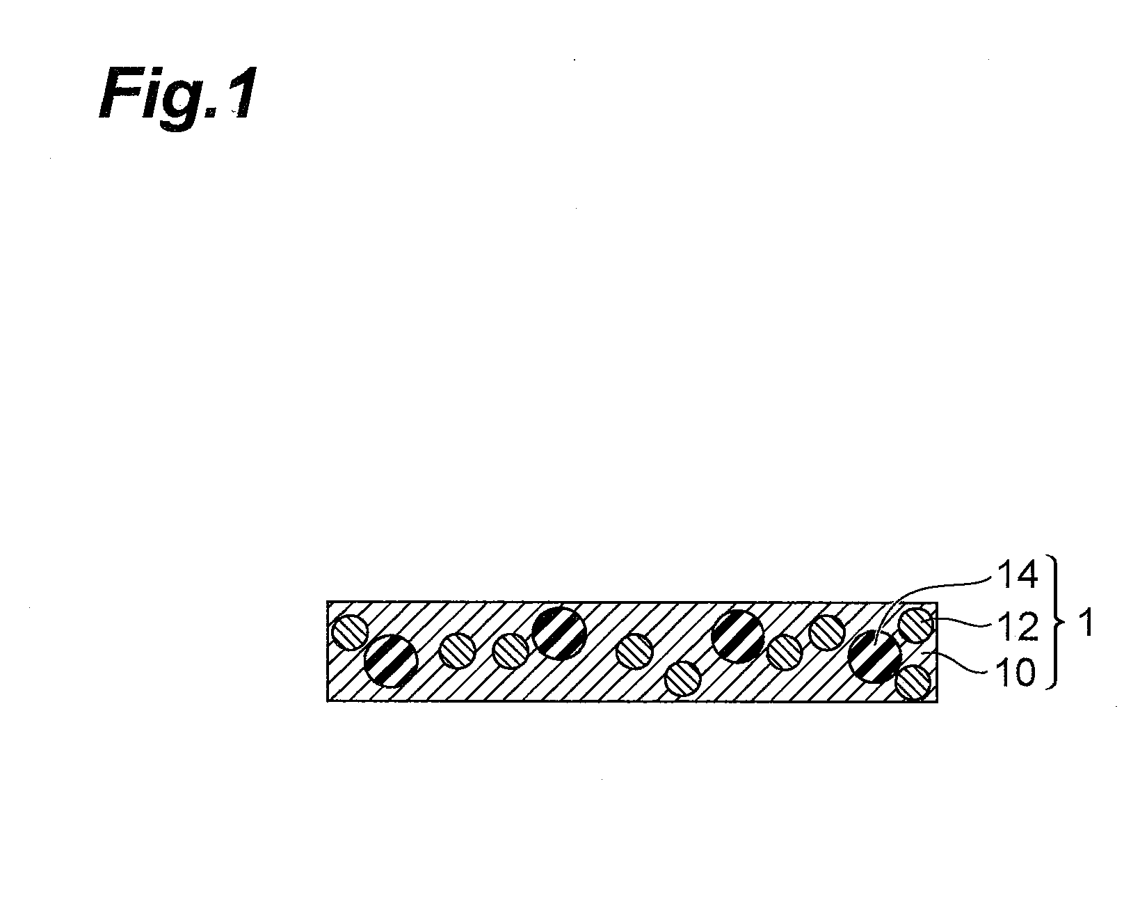
[0012]The circuit connecting adhesive film of the invention preferably comprises the non-conductive phase at 1-60 parts by weight with respect to 100 parts by weight of the insulating adhesive. The melting point of the non-conductive phase is preferably 100-250° C. The non-conductive phase preferably dissolves in the insulating adhesive when the circuit connecting adhesive film has been heated and pressed. If the circuit-connecting material satisfies at least one of these conditions, the effect of the invention will be even more prominently exhibited.
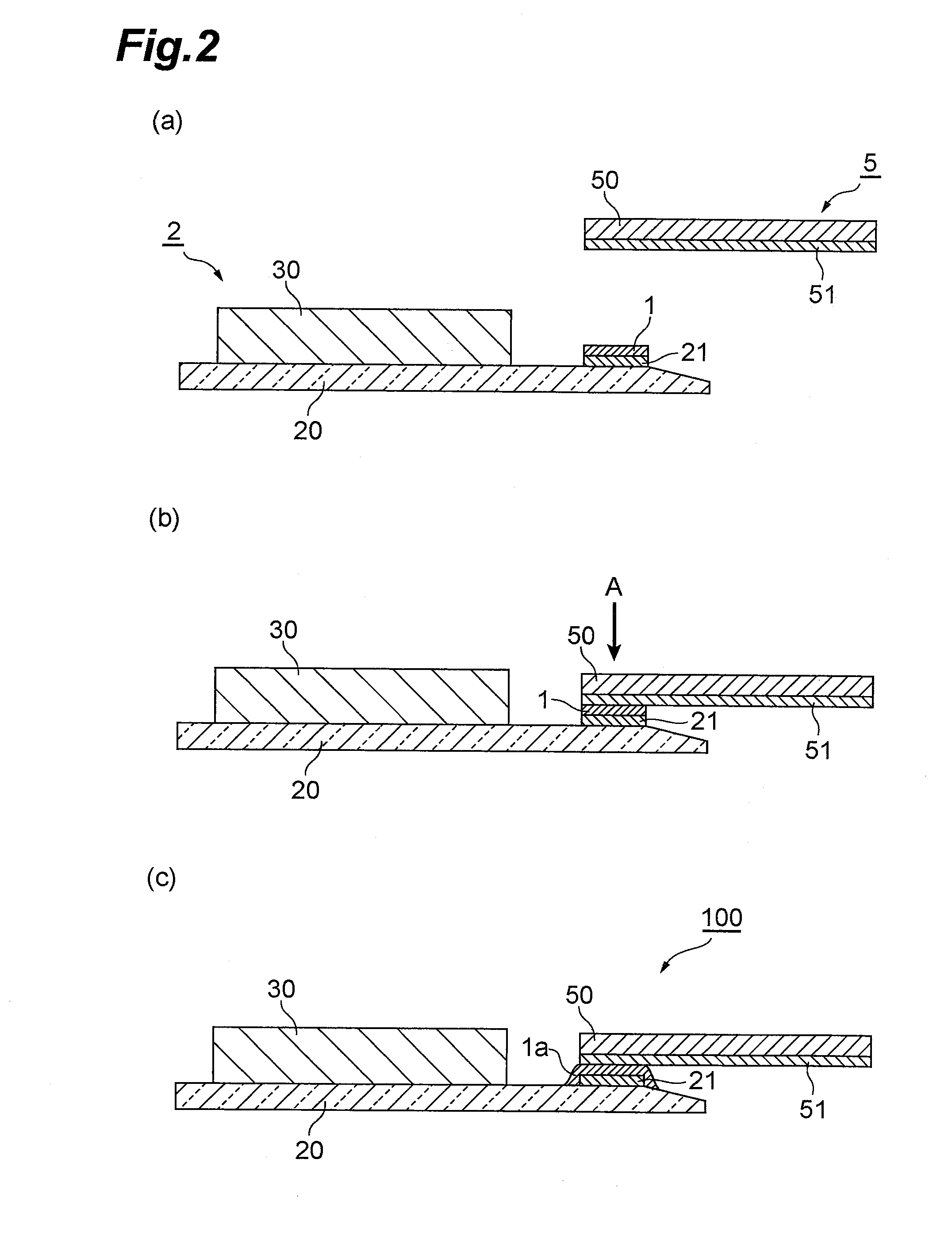
[0013]According to another aspect, the invention relates to a circuit connecting structure comprising a first circuit member with a first connecting terminal, a second circuit member with a second connecting terminal that is laid facing and electrically connected to the first connecting terminal, and an adhesive layer situated between the first circuit member and second circuit member and bonding them. The adhesive layer in the circuit connecting structure of the invention is a layer that can be formed by heating and pressing the circuit connecting adhesive film of the invention that has been situated between the first circuit member and second circuit member.
[0014]According to the circuit connecting structure of the invention, shorting between adjacent circuits is prevented while visibility of impressions on electrode surfaces by conductive particles is satisfactory, and generation of voids after connection is also adequately inhibited.EFFECT OF THE INVENTION
[0015]According to the invention it is possible to obtain satisfactory visibility of impressions on electrode surfaces by conductive particles while preventing shorting between adjacent circuits, and also to prevent generation of voids after connection.

Problems solved by technology

With the employment of COFs and increasingly finer pitches of circuits in LCD modules in recent years, shorting between adjacent electrodes connected using circuit-connecting materials is becoming a more notable problem.

Method used


Image

  • Circuit connecting adhesive film and circuit connecting structure
  • Circuit connecting adhesive film and circuit connecting structure
  • Circuit connecting adhesive film and circuit connecting structure

Examples


example 1

[0069]After combining 20 parts by weight of the radical-polymerizing substance urethane acrylate (trade name: UA-5500T, product of Shin-Nakamura Chemical Co., Ltd.), 20 parts by weight of bis(acryloxyethyl) isocyanurate (trade name: M-215, product of ToaGosei Co., Ltd.), 10 parts by weight of dimethyloltricyclodecane diacrylate (trade name: DCP-A, product of Kyoeisha Chemical Co., Ltd.), 1 part by weight of 2-methacryloyloxyethyl acid phosphate (trade name: P-2M, product of Kyoeisha Chemical Co., Ltd.), 3 parts by weight of benzoyl peroxide (trade name: NYPER BMT-K, product of NOF Corp.) as the free radical generator and 50 parts by weight of a 40 wt % solution of a polyester-urethane resin (trade name: UR8240, product of Toyobo, Ltd.) in a toluene / methyl ethyl ketone=50 / 50 mixed solvent, the mixture was stirred to obtain an insulating adhesive solution.

[0070]To this solution there were added and dispersed 3 vol % of conductive particles with respect to the insulating adhesive, and ...

examples 2-5

[0072]A tape-like circuit-connecting material was fabricated in the same manner as Example 1, except that the types and amounts of non-conductive particles were changed as shown in Table 1. The non-conductive particles used in Example 2 were polyamide-based elastomer particles (mean particle size: 10 μm, 10% compression modulus (K value): 260 Kgf / mm2, melting point: 170° C.), the non-conductive particles used in Example 3 were polyamide-based elastomer particles (mean particle size: 5 μm, 10% compression modulus (K value): 270 Kgf / mm2, melting point: 180° C.), the non-conductive particles used in Example 4 were polyamide-based elastomer particles (mean particle size: 3 μm, 10% compression modulus (K value): 280 Kgf / mm2, melting point: 200° C.), and the non-conductive particles used in Example 5 were polyester-based elastomer particles (mean particle size: 5 μm, 10% compression modulus (K value): 290 Kgf / mm2, melting point: 210° C.).


PUM

PropertyMeasurementUnit
Percent by massaaaaaaaaaa
Melting pointaaaaaaaaaa

Abstract

A circuit connecting adhesive film comprising an insulating adhesive, conductive particles and a particulate non-conductive phase containing a polyamide-based elastomer and / or a polyester-based elastomer, wherein the conductive particles and non-conductive phase are dispersed in the insulating adhesive.

Description

TECHNICAL FIELD[0001]The present invention relates to a circuit connecting adhesive film and a circuit connecting structure.BACKGROUND ART[0002]Circuit-connecting materials, used for heating and pressing of circuit boards with mutually opposing electrodes for electrical connection between electrodes in the pressing direction, include anisotropic conductive adhesive films comprising conductive particles dispersed in epoxy-based adhesives or acrylic adhesives, for example. Anisotropic conductive adhesive films are widely used for electrical connection between liquid crystal display (LCD) panels and TCP (Tape Carrier Package) or COF (Chip On Flex) members on which are mounted mainly semiconductor chips that drive the LCDs, and between TCPs or COFs and printed circuit boards.[0003]Recently, flip-chip mounting, which is advantageous for thickness reduction and narrow-pitch connection, has come to be employed instead of wire bonding methods even when semiconductor chips are mounted face-d...

Claims


Application Information

Patent Timeline
IPC IPC(8): B32B7/12B32B5/08
CPCH05K3/323Y10T428/28H05K2201/0212H05K2201/0133C08J5/18
Inventor TATSUZAWA, TAKASHIKOBAYASHI, KOUJIITO, AKIHIROYOKOZUMI, TOMOMI
Owner HITACHI CHEM CO LTD
Why Eureka
Eureka Blog
Learn More