

Structure stamp, device and method of embossing
- Summary
- Abstract
- Description
- Claims
- Application Information
AI Technical Summary
Benefits of technology
Problems solved by technology
Method used
Image

Examples
Embodiment Construction
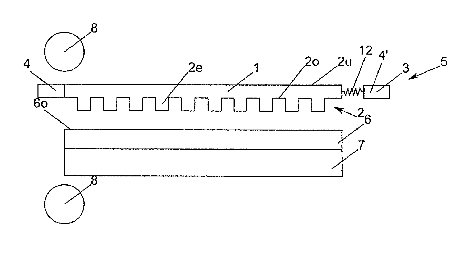
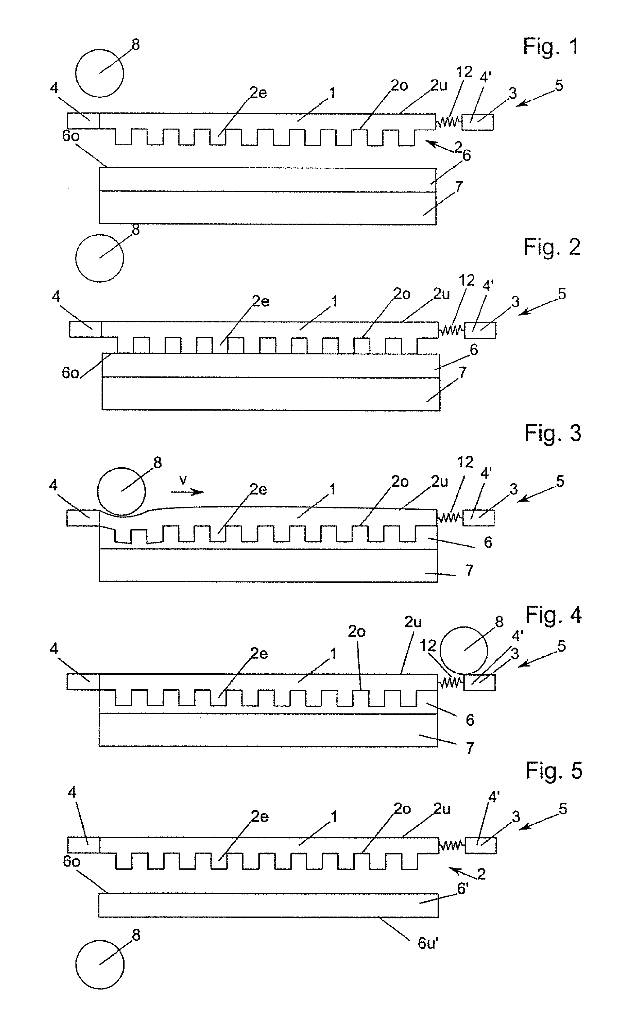
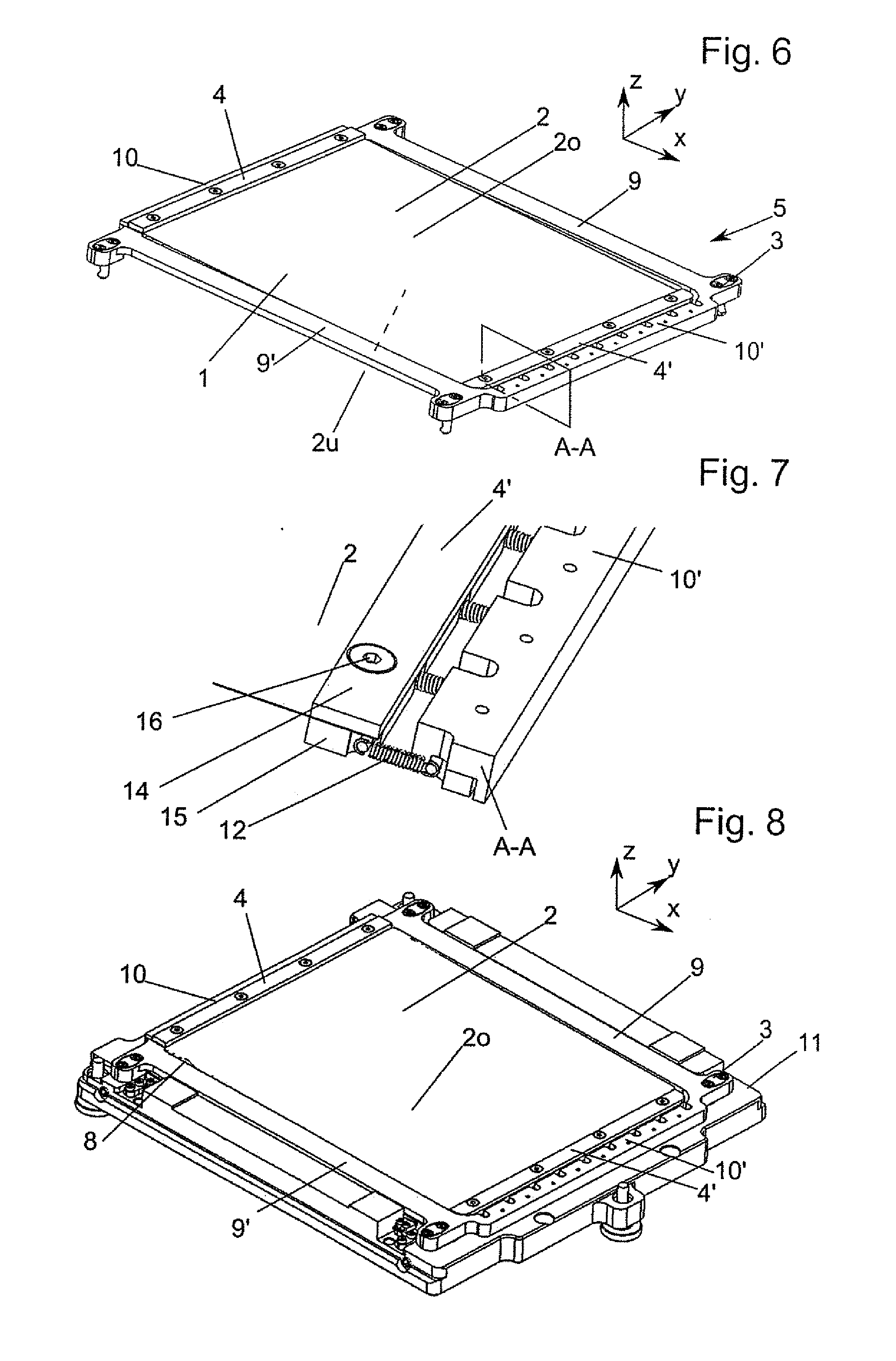
[0047]In the figures, advantages and features of the invention are labeled with the reference numbers which identify them according to embodiments of the invention, components or features with the same function or function with the same effect being labeled with identical reference numbers.
[0048]In the figures, the features in FIGS. 1 to 5 are not shown to scale, in order to be able to represent the operation of the individual features at all. The ratios of the individual components are in part also disproportionate; this can be attributed especially to nanostructures 2e which are shown highly enlarged. The nanostructures 2e, which are embossed with this invention or which are used for embossing of corresponding nanostructures onto workpieces, are in the nanometer and / or micron range, while the magnitude of the size of the machine components is in the centimeter range.
[0049]The dimensions of the individual nanostructures 2e of the embossing pattern 2 are preferably in the micron ran...
PUM
| Property | Measurement | Unit |
|---|---|---|
| Force | aaaaa | aaaaa |
| Flexibility | aaaaa | aaaaa |
Abstract
Description
Claims
Application Information