

device
a technology of test circuits and chips, applied in the field of devices, can solve the problems of insufficient acquisition of advantages of chip test using test circuits incorporated in chips, such as a higher-speed chip test and a lower cost of chip test, and achieve the effects of increasing the area of the test circuit in the device, improving the quality of the chip test, and increasing the size of the test circui
- Summary
- Abstract
- Description
- Claims
- Application Information
AI Technical Summary
Benefits of technology
Problems solved by technology
Method used
Image

Examples
embodiment 1
[0049]In this embodiment, a structure example of one embodiment of the present invention is described.
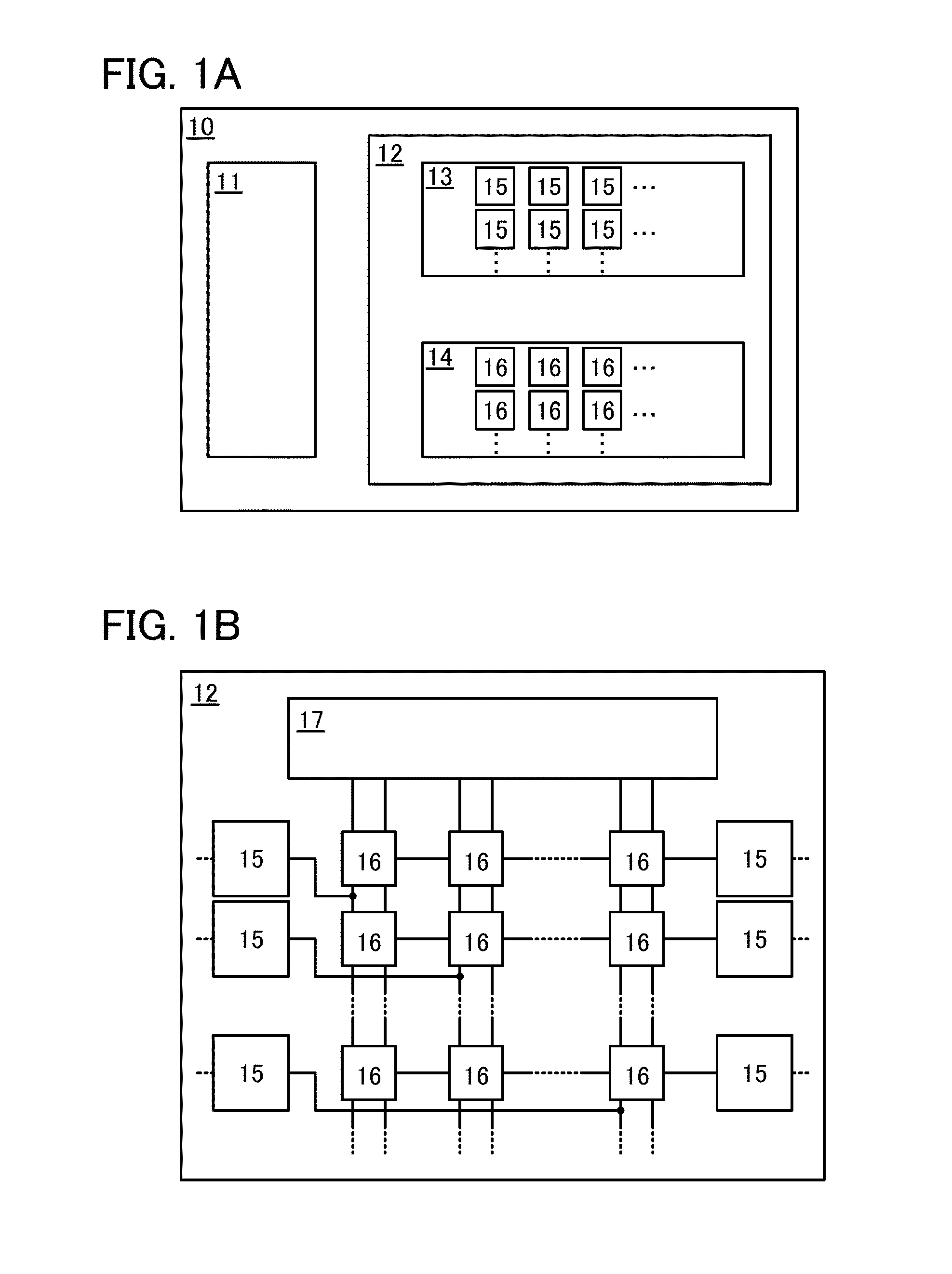
[0050]FIGS. 1A and 1B illustrate a structure example of a device according to one embodiment of the present invention. A device 10 in FIG. 1A includes a circuit 11 and a circuit 12. The circuit 11 is a circuit having an arithmetic function, a control function, and the like, typically an integrated circuit including a plurality of transistors. The circuit 11 includes a variety of logic circuits such as a sequential circuit or a combination circuit and can be used as a central processing device. The circuit 12 is typically, like the circuit 11, an integrated circuit including a plurality of transistors, preferably a circuit whose circuit configuration is reconfigurable (hereinafter also referred to as reconfiguration circuit).
[0051]The circuit 12 includes a circuit 13 and a circuit 14. The circuit 13 includes a plurality of circuits 15 (hereinafter also referred to as programmable log...
embodiment 2
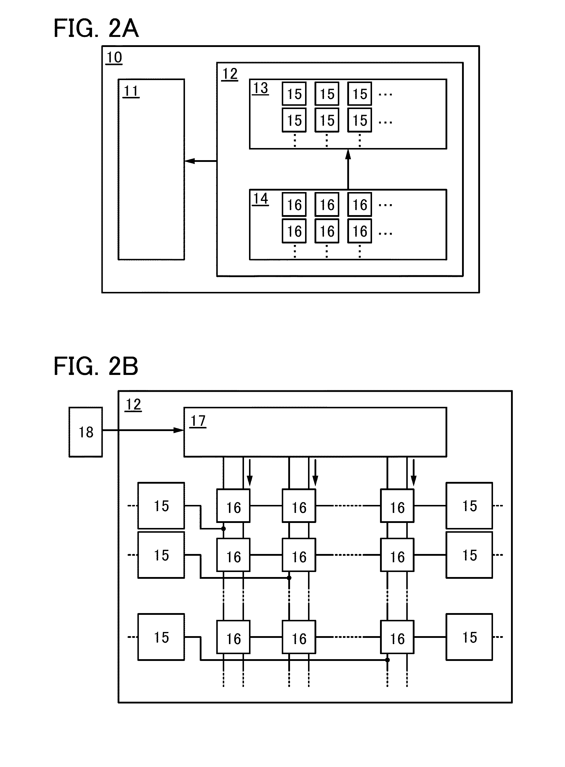
[0086]In this embodiment, a specific configuration example of the circuit 12 in FIGS. 1A and 1B to FIGS. 3A and 3B is described.
[0087]FIG. 6 shows an example of a configuration of the circuit 12. The circuit 12 includes a cell array 30 including the plurality of PLEs 15 and the plurality of SWs 16, the circuit 17, a circuit 41, and a circuit 42. Note that the plurality of SWs 16 is each connected to the circuits 17, 41, and 42. The plurality of PLEs 15 is each connected to at least one of the SWs 16.
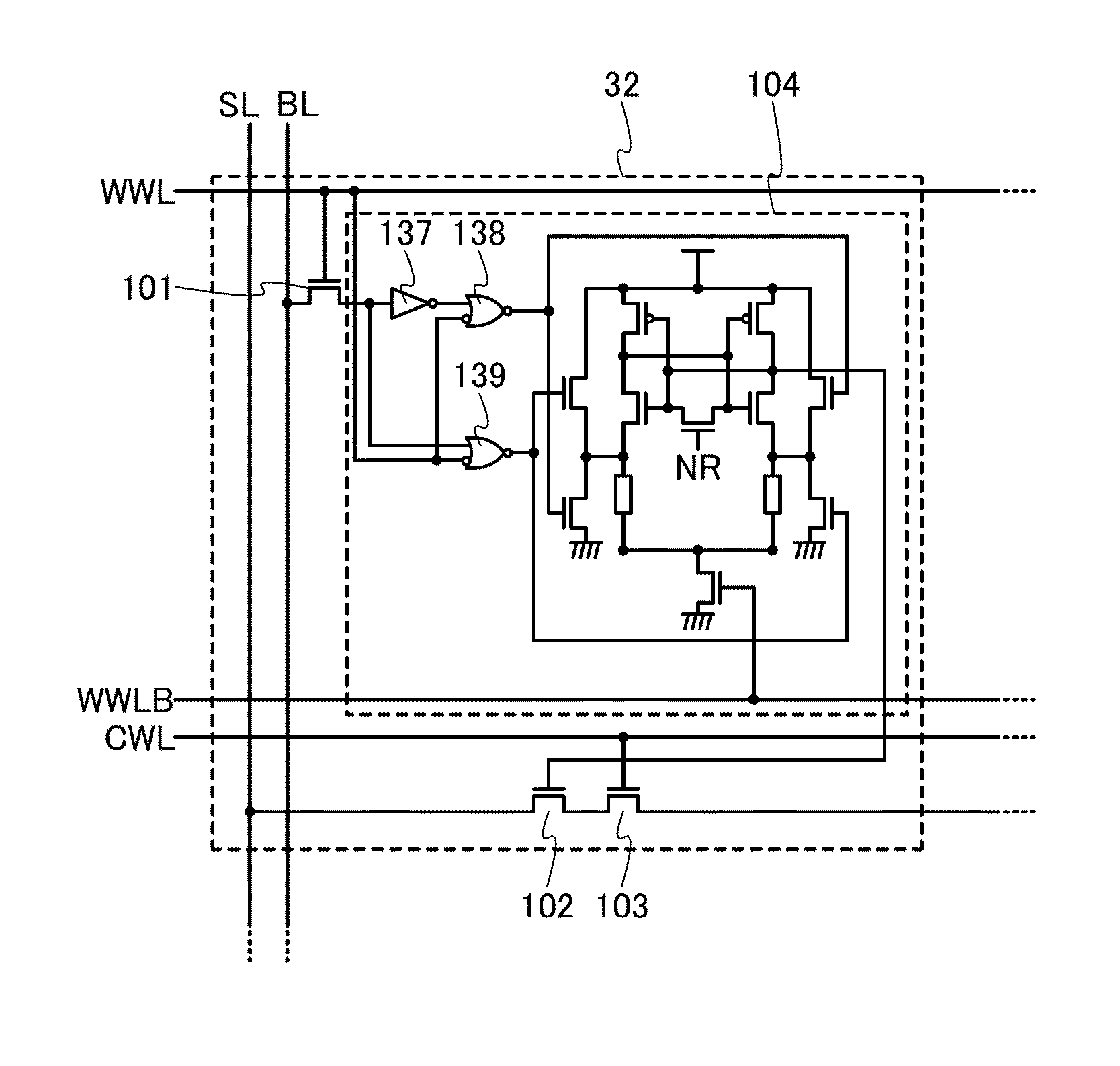
[0088]The SW 16 includes cells 32 in x rows, and the cell array 31 includes the SWs 16 in y columns. A cell array 30 includes cell arrays 31 in s rows and thus includes (sx×y) cells 32. Each of the cells 32 stores data output from the circuit 17.
[0089]In the case where the circuit 12 is used as a test circuit, configuration data are output from the circuit 17 and stored in the cells 32. The conduction of the cell 32 is controlled in accordance with the configuration data, and the circuit...
embodiment 3
[0175]In this embodiment, a specific structure example of the circuit 43 in FIG. 7 is described.
[0176]FIG. 12 shows a configuration example of the circuit 43. The circuit 43 includes a shift register 200, selection circuits 204 to 206, a line buffer including latch circuits 207 to 212, transistors 213 to 221, and enable buffers 222 to 224.
[0177]The shift register 200 includes latch circuits 201 to 203. A start pulse supplied through the wiring SP and a clock signal supplied through the wiring CK are input to the latch circuit 201. An input terminal and an output terminal of the latch circuit 201 are connected to input terminals of an AND circuit. An output terminal of the AND circuit is connected to a wiring SEL[1]. An output signal of the latch circuit 201 and an inverted clock signal supplied through the wiring CKB are input to the latch circuit 202. An input terminal and an output terminal of the latch circuit 202 are connected to input terminals of an AND circuit. An output term...
PUM
 Abstract
Description
Claims
Application Information