Display panel and display device

a display panel and display device technology, applied in semiconductor devices, instruments, electrical devices, etc., can solve the problems of high heat resistance, inability to apply to the panel requiring high fineness, and inability to meet the application requirements of large-size or flexible substrates, so as to achieve less covering width, stable tft efficiency, and less covering width

Active Publication Date: 2015-08-27
INNOLUX CORP
View PDF1 Cites 12 Cited by
  • Summary
  • Abstract
  • Description
  • Claims
  • Application Information

AI Technical Summary

Benefits of technology

[0014]As mentioned above, in the display panel and display device of the invention, the first insulating layer of the TFT substrate includes a first sub-layer and a second sub-layer disposed on the drain of the TFT sequentially. The first sub-layer has a first opening having a first width. The second sub-layer has a second opening having a second width on the first opening. The first opening and the second opening can form a first via, and the second width can be greater than the first width. The pixel electrode layer of the TFT substrate is disposed on the second insulating layer and disposed in the first via to connect the drain. In comparison with the conventional art, by the first sub-layer and second sub-layer sequentially disposed on the drain of the TFT, the efficiency of the TFT can be kept stable after a period of time of the operation and therefore the display quality of the display panel and display device won't be affected.
[0015]Besides, in an embodiment of the invention, the projections of the first via formed by the first opening and the second opening and the second via of the passivation layer on the substrate of the TFT substrate overlap each other, and the area of the overlap can be between 4 μm2 and 49 μm2. Thereby, in comparison with the conventional art where another via is formed by etching the greater via, the area of the overlap of the first via and the second via can be less than that of the via of the conventional art, and the alignment issue between the greater via and the another via in the greater via will be avoided. Moreover, since the area of the overlap is less than that of the via of the conventional art, the black matrix disposed on the scan line will have a less covering width than the conventional art and the pixel aperture of the display panel and display device can be thus increased.

Problems solved by technology

However, it needs to be made under the environment of over 450° C., so it only can be formed on the substrate with high heat resistance and is not suitable for the application of large-size or flexible substrate.
Besides, although the conventional amorphous TFT can be formed under the environment of lower temperature, e.g. about 300° C., this kind of amorphous TFT only has carrier mobility of about 1 cm2 / Vs, so it can't be applied to the panel requiring high fineness.
Therefore, the efficiency of the TFT will be reduced and the display quality of the display panel and display device will be thus affected.

Method used


Image

  • Display panel and display device
  • Display panel and display device
  • Display panel and display device

Examples


Embodiment Construction

[0030]The present invention will be apparent from the following detailed description, which proceeds with reference to the accompanying drawings, wherein the same references relate to the same elements.

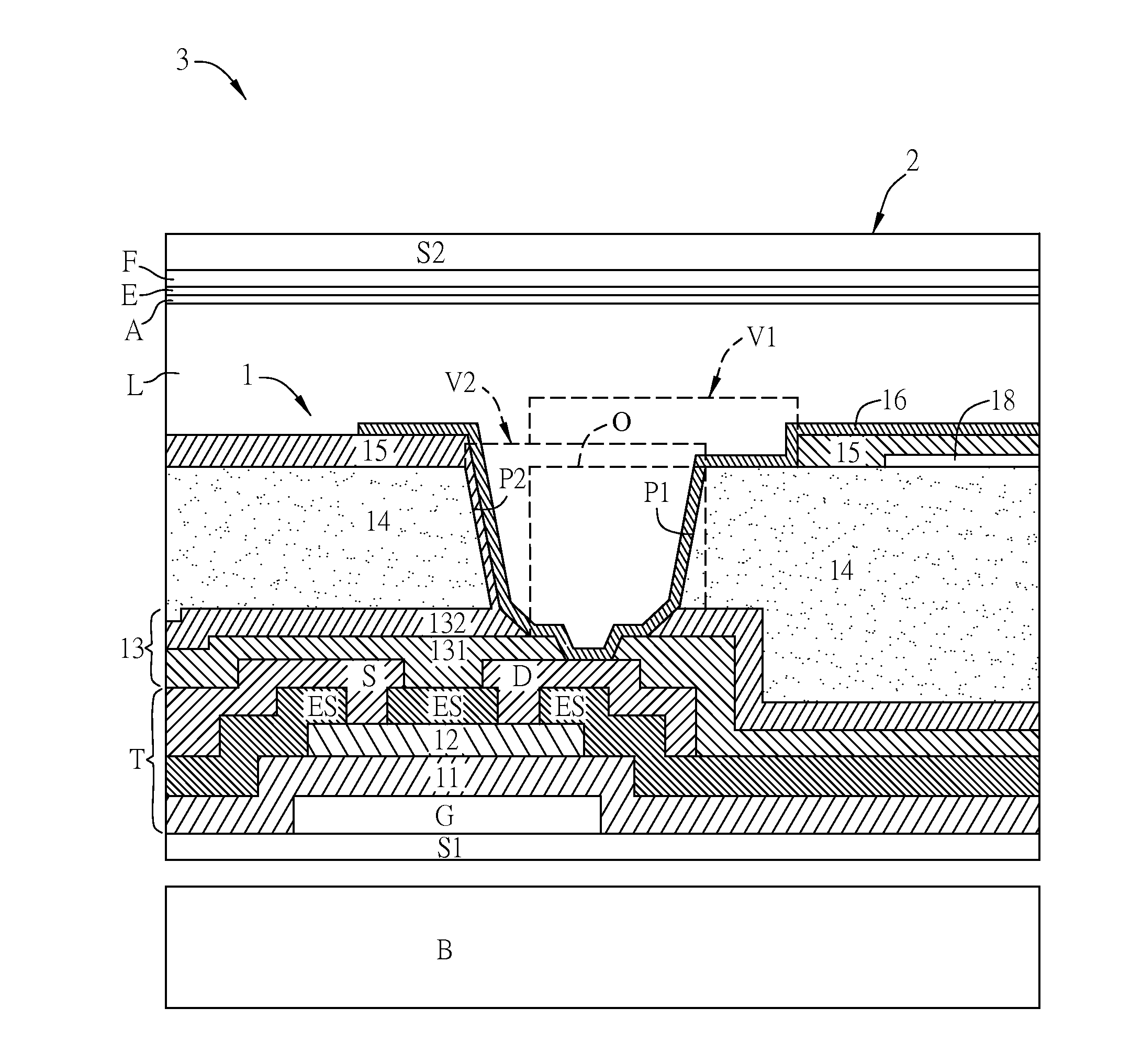
[0031]The display panel of an embodiment of the invention is an active matrix LCD panel and includes a TFT substrate 1. As below, the structure of the TFT substrate 1 is illustrated first.

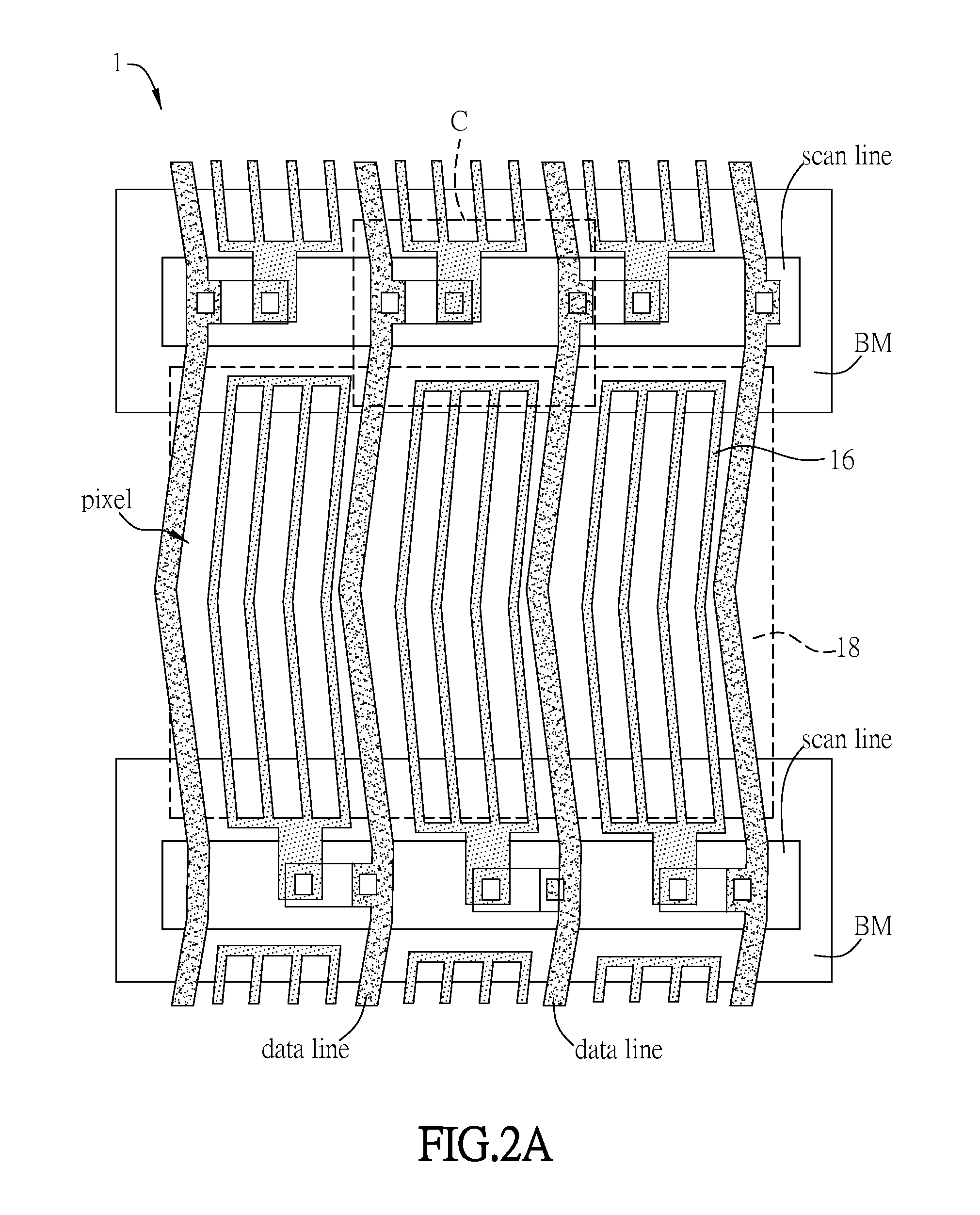
[0032]FIG. 2A is a schematic top-view diagram of the TFT substrate 1, FIG. 2B is a schematic enlarged diagram of the region C in FIG. 2A, FIG. 2C is a schematic sectional diagram taken along the line B-B in FIG. 2B, and FIG. 2D is a schematic enlarged diagram of a part of FIG. 2C. To be noted, for the convenient illustration, the size relation (e.g. ratio) of the height and width of each element shown in FIGS. 2A to 2D is just for the illustrative purpose but not for representing the real one.

[0033]As shown in FIG. 2A, the TFT substrate 1 can include a plurality of scan lines, a plurality of data lin...


PUM

PropertyMeasurementUnit
sizeaaaaaaaaaa
sizeaaaaaaaaaa
distanceaaaaaaaaaa

Abstract

A display panel includes a TFT substrate, an opposite substrate and a display layer. A TFT of the TFT substrate has a drain. A first insulating layer has a first sub-layer and a second sub-layer disposed on the drain sequentially. The first sub-layer has a first opening with a first width. The second sub-layer has a second opening with a second width on the first opening. The first and second openings form a first via, and the second width is greater than the first width. A passivation layer is disposed on the first insulating layer. A second insulating layer is disposed on the passivation layer. A pixel electrode layer is disposed on the second insulating layer and disposed in the first via to connect the drain. The display layer is disposed between the TFT substrate and the opposite substrate.

Description

CROSS REFERENCE TO RELATED APPLICATIONS[0001]This Non-provisional application claims priority under 35 U.S.C. §119(a) on Patent Application No(s). 103106290 filed in Taiwan, Republic of China on Feb. 25, 2014, the entire contents of which are hereby incorporated by reference.BACKGROUND OF THE INVENTION[0002]1. Field of Invention[0003]The invention relates to a display panel and a display device having the display panel.[0004]2. Related Art[0005]With the progress of technologies, flat display devices have been widely applied to various kinds of fields. Especially, liquid crystal display (LCD) devices, having advantages such as compact structure, low power consumption, less weight and less radiation, gradually take the place of cathode ray tube (CRT) display devices, and are widely applied to various electronic products, such as mobile phones, portable multimedia devices, notebooks, LCD TVs and LCD screens.[0006]A conventional LCD device includes a thin film transistor (TFT) substrate...

Claims


Application Information

Patent Timeline
Patent Type & Authority Applications(United States)
IPC IPC(8): H01L27/12G02F1/1333G02F1/1368G02F1/1362H01L29/786H01L27/32
CPCH01L27/1248H01L27/124H01L29/78618H01L29/7869G02F1/133345H01L27/3276H01L27/3248G02F1/1368G02F1/136227H01L27/3258H01L27/1225H10K50/841H10K59/123H10K59/124H10K59/131H10K59/1213H10K2102/00H10K2102/351G02F1/136286
Inventor LEE, KUAN-FENGWANG, HUI-CHIEH
Owner INNOLUX CORP
Why Eureka
Try Eureka