
Front-side emitting mid-infrared light emitting diode

Active Publication Date: 2015-08-27
TERAHERTZ DEVICE
View PDF10 Cites 5 Cited by
  • Summary
  • Abstract
  • Description
  • Claims
  • Application Information

AI Technical Summary

Benefits of technology

This patent describes a system for generating mid-infrared LEDs that are brighter than existing options. The LEDs use a semiconductor substrate of gallium antimonide or related materials, and can include epitaxial heterostructures of different materials to create light emitting structures. These LEDs can be configured into a high-brightness LED die and can also include optical power conversion superlattices for more efficient light emission. The technical effects of this patent include brighter and more powerful mid-infrared LEDs that can be used in various applications such as optical communication or imaging.

Problems solved by technology

However, there are not corresponding mid-infrared high-brightness LEDs, which might take advantage of this technology base, and there are not corresponding mid-infrared high-brightness LEDs with their own supporting specialized industrial technology base.

Method used


Image

  • Front-side emitting mid-infrared light emitting diode
  • Front-side emitting mid-infrared light emitting diode
  • Front-side emitting mid-infrared light emitting diode

Examples


Embodiment Construction

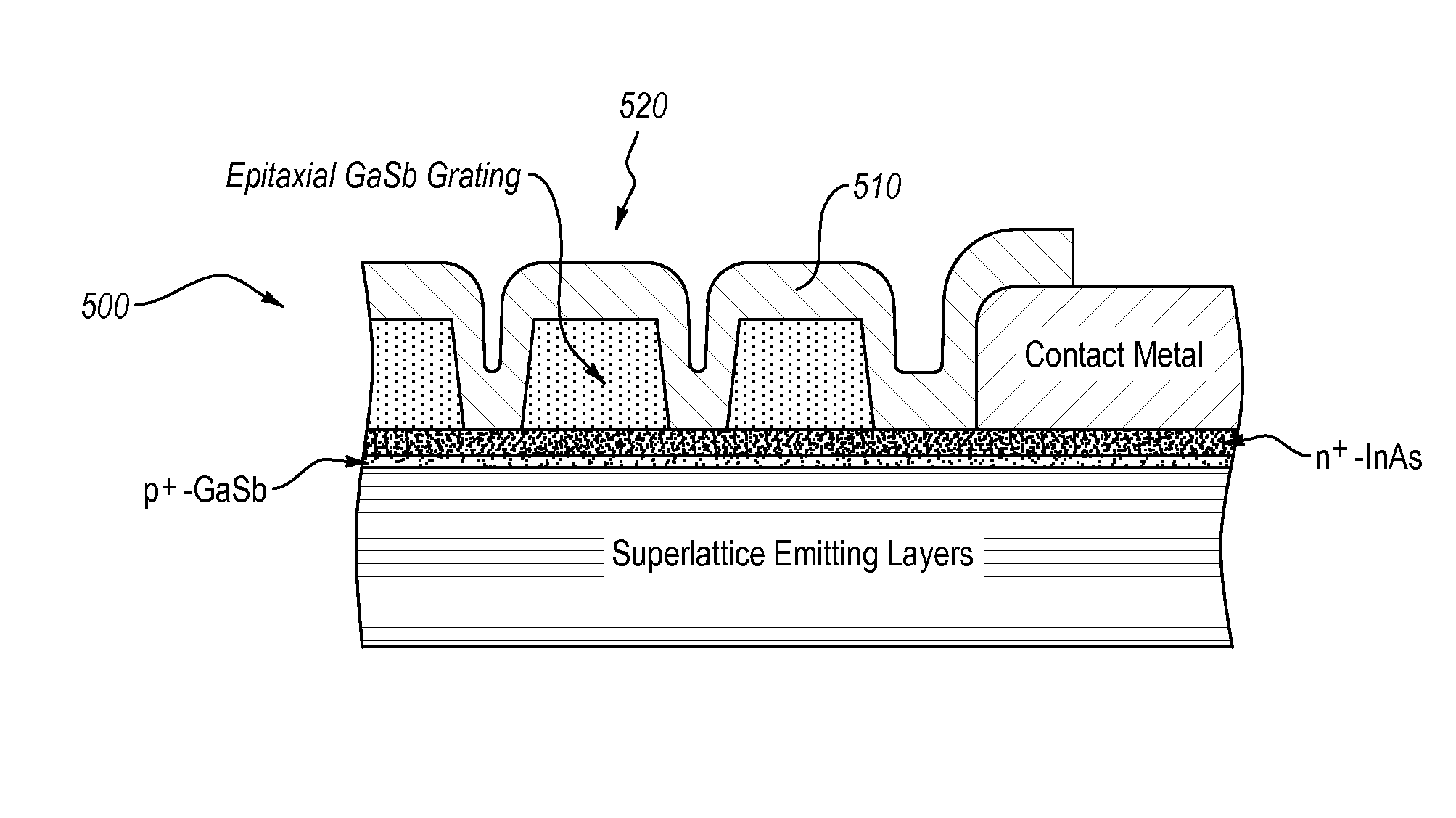
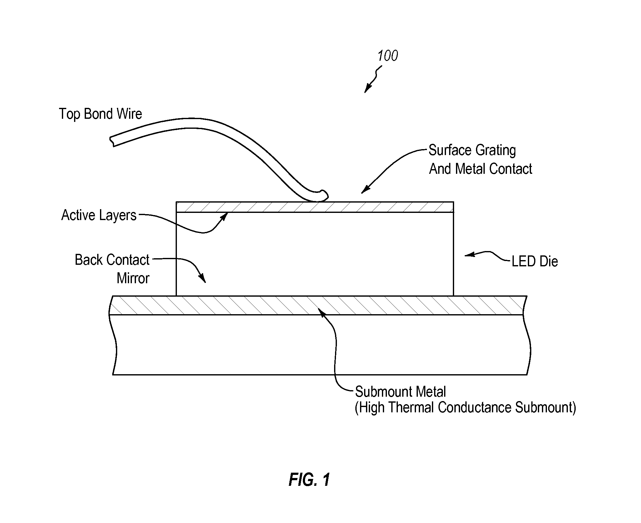
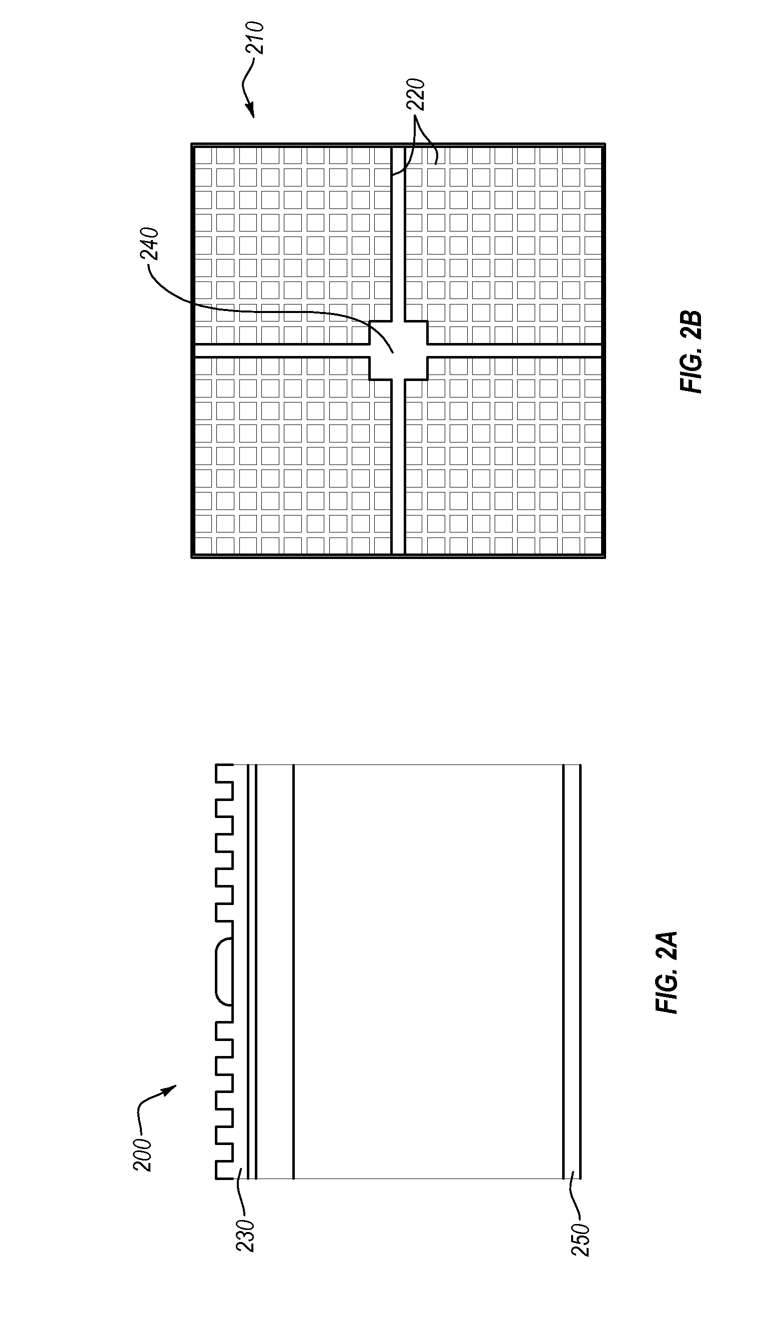
[0030]The present invention extends to systems, methods, and apparatus configured to generate mid-infrared LEDs. In particular, embodiments of the present invention comprise mid-infrared high-brightness LEDs that are configured to take advantage of one or more existing support technologies. Additionally, embodiments of the present invention provide unique and novel configurations for LED devices.

[0031]The embodiments disclosed herein of the present mid-infrared LEDs include devices with wavelengths that range from about 3 to 20 μm. In at least one embodiment of the present invention, particular wavelengths of light can be obtained by making specific adjustments to the antimonide-arsenide semiconductor hetero structure layer thicknesses and by making specific adjustments to the sizes of the light-extraction buttes on the surface and to the thicknesses of the anti-reflection coating. In at least one embodiment, the mechanical, electrical, optical, and packaging features and structures...


PUM


Abstract

A device emitting mid-infrared light that comprises a semiconductor substrate of GaSb or closely related material. The device can also comprise epitaxial heterostructures of InAs, GaAs, AlSb, and related alloys forming light emitting structures cascaded by tunnel junctions. Further, the device can comprise light emission from the front, epitaxial side of the substrate.

Description

CROSS-REFERENCE TO RELATED APPLICATIONS[0001]This application claims priority to and the benefit of U.S. Provisional Application Ser. No. 61 / 942,932, entitled “Front-side Emitting Mid-Infrared Light Emitting Diode,” filed on Feb. 21, 2014, which application is incorporated by reference in its entirety herein.BACKGROUND OF THE INVENTION[0002]1. Technical Field[0003]The embodiments disclosed herein are related to the field of light emitting diode (LED) devices.[0004]2. Background and Relevant Art[0005]Unless otherwise indicated herein, the materials described in this section are not prior art to the claims in this application and are not admitted to be prior art by inclusion in this section. The use of the term “background” is inclusive of the term “context.” Thus, the following section provides both context for the disclosure and may also provide patentable support for the claims.[0006]The use of doped semiconductors to create barriers, injectors, tunnel junction contacts, cascade LE...

Claims


Application Information

Patent Timeline
IPC IPC(8): H01L33/06H01L33/30H01L33/60H01L33/62H01L33/46H01L33/00H01L33/38
CPCH01L33/06H01L33/0025H01L33/30H01L33/60H01L33/62H01L33/46H01L33/38H01L24/05H01L2224/487H01L33/0062H01L33/04H01L33/40H01L2933/0016H01L2933/0025H01L2224/48091H01L2224/04042H01L33/0093H01L2924/00014
Inventor MILLER, MARK S.
Owner TERAHERTZ DEVICE
Features
  • Generate Ideas
  • Intellectual Property
  • Life Sciences
  • Materials
  • Tech Scout
  • Unparalleled Data Quality
  • Higher Quality Content
  • 60% Fewer Hallucinations
Learn More