Method for manufacturing display device and method for manufacturing electronic device

a display device and electronic device technology, applied in the field of display devices, can solve the problems of reducing reliability and manufacturing yield of display devices, easily damaged electrodes in display devices, etc., and achieve the effects of high reliability, not easily damaged electrodes, and not easily damaged display regions

Active Publication Date: 2015-09-03
SEMICON ENERGY LAB CO LTD
View PDF0 Cites 40 Cited by
  • Summary
  • Abstract
  • Description
  • Claims
  • Application Information

AI Technical Summary

Benefits of technology

[0020]One embodiment of the present invention provides a method for manufacturing a display device, which does not easily damage an electrode. One embodiment of the present invention provides a method for manufacturing a display device, which does not easily damage a display region. One embodiment of the present invention provides a highly reliable display device and a method for manufacturing the display device.
[0021]One embodiment of the present invention provides a display device, electronic device, or the like havi

Problems solved by technology

However, a method in which part of a flexible substrate is removed by a laser beam or with an edged tool has a problem in that an electr

Method used


Image

  • Method for manufacturing display device and method for manufacturing electronic device
  • Method for manufacturing display device and method for manufacturing electronic device
  • Method for manufacturing display device and method for manufacturing electronic device

Examples


embodiment 1

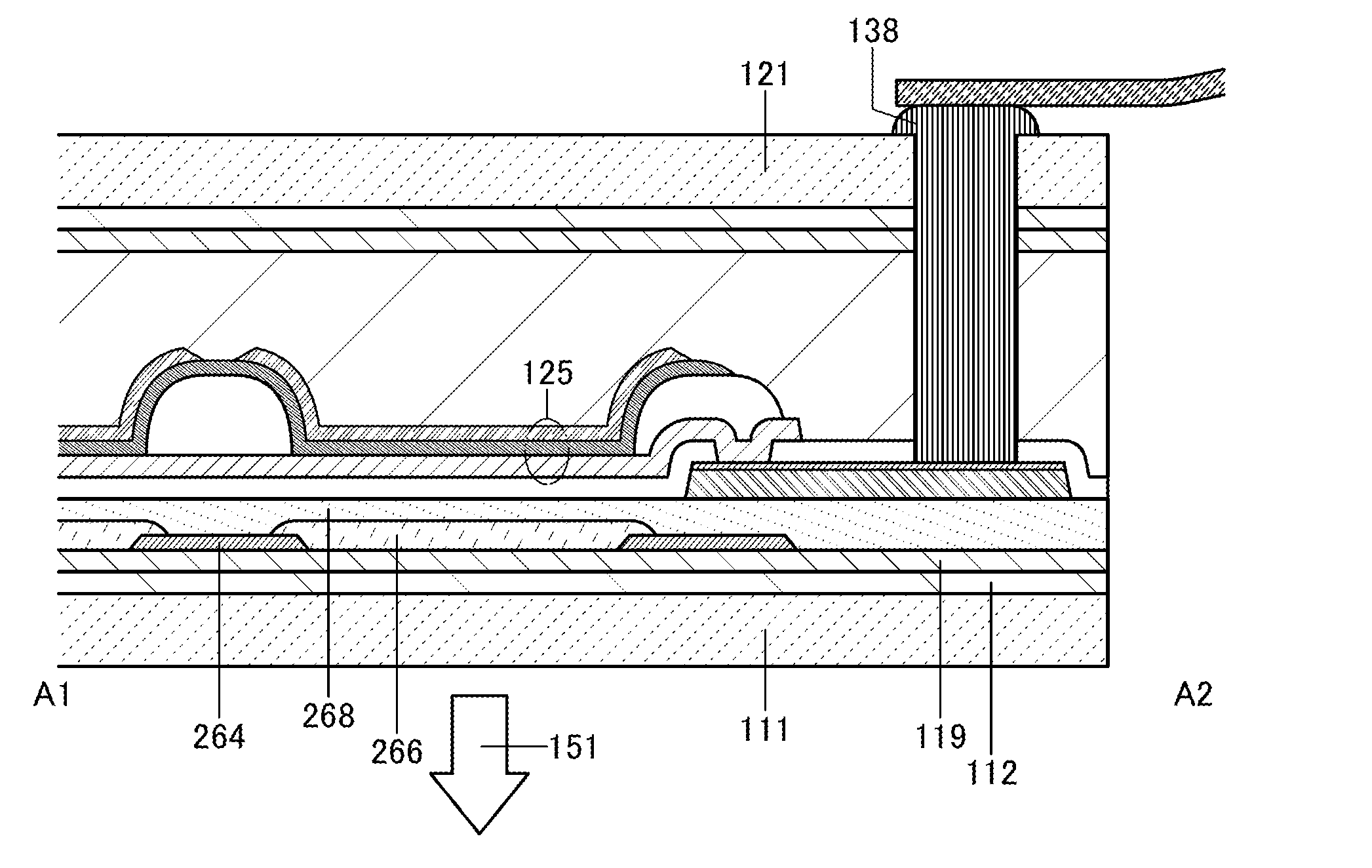
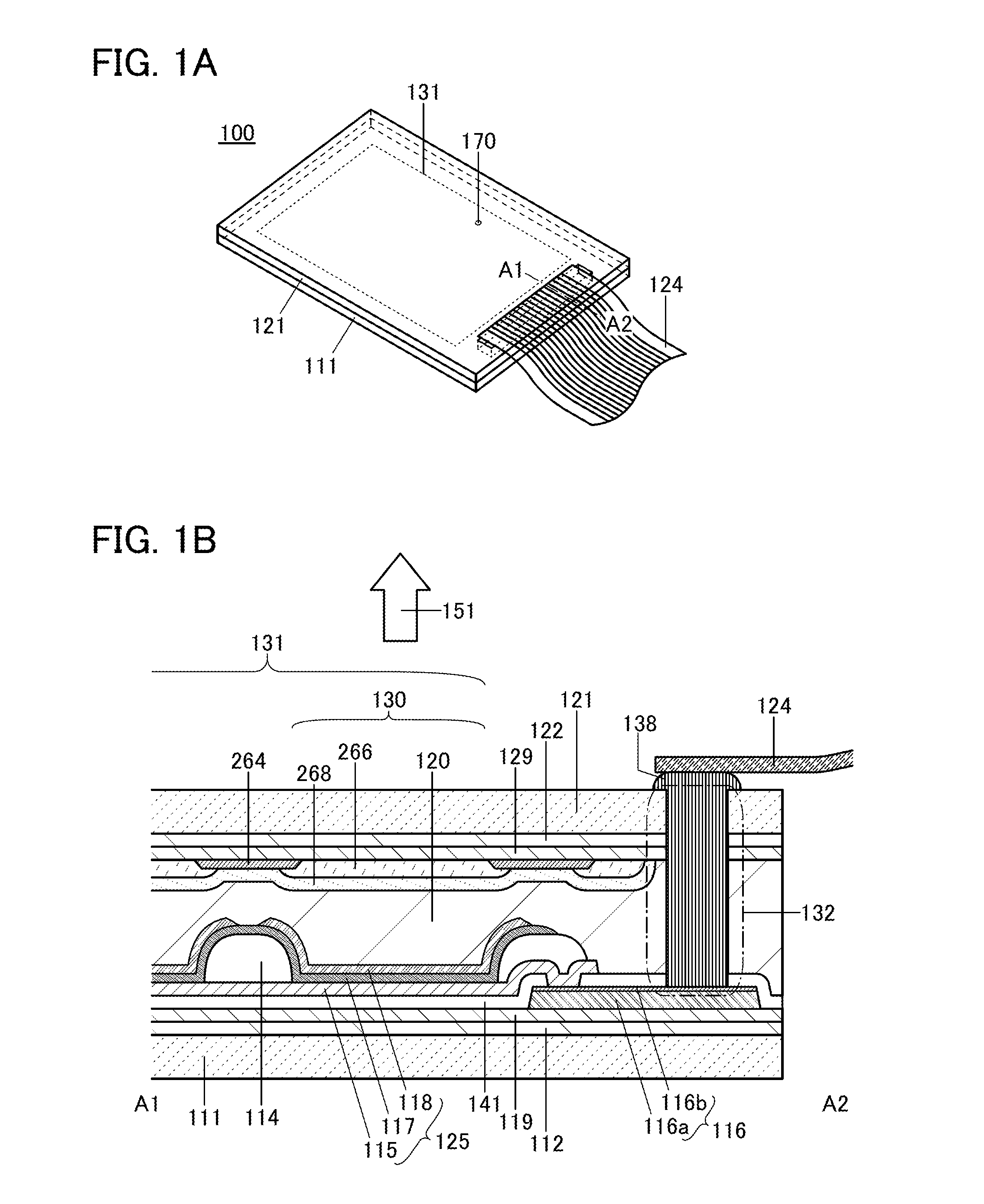
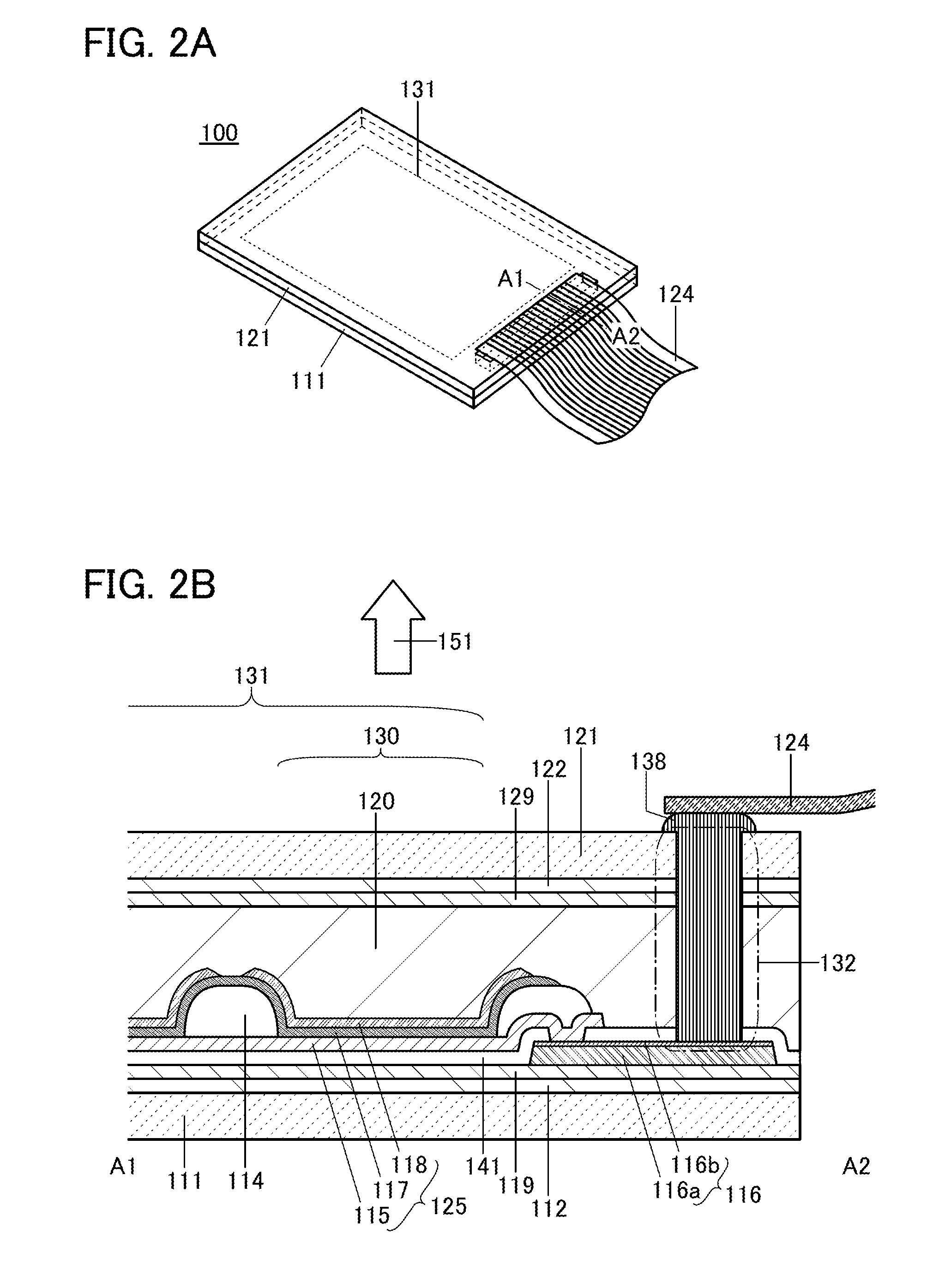
[0085]A structure example of a display device 100 of one embodiment of the present invention will be described with reference to FIGS. 1A and 1B, FIGS. 2A and 2B, FIGS. 3A and 3B, FIGS. 4A to 4E, FIGS. 5A to 5D, FIGS. 6A to 6F, FIGS. 7A to 7C, FIGS. 8A and 8B, FIGS. 9A and 9B, FIGS. 10A and 10B, FIGS. 11A and 11B, FIGS. 12A and 12B, and FIGS. 13A and 13B. FIG. 1A is a perspective view of the display device 100 to which an external electrode 124 is connected, and FIG. 1B is a cross-sectional view taken along the dashed-dotted line A1-A2 in FIG. 1A. Note that the display device 100 disclosed in this specification is a display device in which a light-emitting element is used as a display element. As the display device 100 of one embodiment of the present invention, a display device having a top-emission structure is described as an example. Note that the display device 100 can be a display device having a bottom-emission structure or a dual-emission structure.

[0086]The display device 1...

embodiment 2

[0197]In this embodiment, a display device 200 having a structure different from the structure of the display device 100 described in the above embodiment will be described with reference to FIGS. 15A and 15B. FIG. 15A is a top view of the display device 200, and FIG. 15B is a cross-sectional view taken along the dashed-dotted line A3-A4 in FIG. 15A.

[0198]The display device 200 described in this embodiment includes a display region 231 and a peripheral circuit 251. The display device 200 further includes the electrode 116 and the light-emitting element 125 including the electrode 115, the EL layer 117, and the electrode 118. A plurality of light-emitting elements 125 are formed in the display region 231. A transistor 232 for controlling the amount of light emitted from the light-emitting element 125 is connected to each light-emitting element 125.

[0199]The electrode 116 is electrically connected to the external electrode 124 through the anisotropic conductive connection layer 138 fo...

embodiment 3

[0234]A structure example of a display device 1100 of one embodiment of the present invention will be described with reference to FIGS. 18A and 18B, FIGS. 19A and 19B, FIGS. 20A and 20B. FIGS. 21A to 21D, FIGS. 22A to 22D, FIGS. 23A to 23C, FIGS. 24A to 24E, FIGS. 25A and 25B, FIGS. 26A and 26B, FIGS. 27A and 27B, FIGS. 28A and 28B, FIGS. 29A and 29B, FIGS. 30A and 30B, and FIGS. 31A to 31C. FIG. 18A is a perspective view of the display device 1100 to which the external electrode 124 is connected, and FIG. 18B is a cross-sectional view taken along the dashed-dotted line A5-A6 in FIG. 18A. The display device 1100 disclosed in this specification is a display device in which a light-emitting element is used as a display element. As the display device 1100 of one embodiment of the present invention, a display device having a top-emission structure is described as an example. Note that the display device 1100 can be a display device having a bottom-emission structure or a dual-emission s...


PUM


Abstract

A method for manufacturing a display device is provided. The method includes forming a display element interposed between a first substrate and a second substrate and peeling the second substrate from the first substrate so that an electrode, which is located between the first and second substrates and to be connected to an external electrode, is exposed simultaneously with the peeling of the second substrate.

Description

BACKGROUND OF THE INVENTION[0001]1. Field of the Invention[0002]The present invention relates to a display device. The present invention also relates to a method for manufacturing the display device.[0003]Note that one embodiment of the present invention is not limited to the above technical field.[0004]Note that in this specification and the like, a semiconductor device generally means a device that can function by utilizing semiconductor characteristics. Thus, a semiconductor element such as a transistor or a diode and a semiconductor circuit are semiconductor devices. A display device, a light-emitting device, a lighting device, an electro-optical device, an electronic device, and the like may include a semiconductor element or a semiconductor circuit. Therefore, a display device, a light-emitting device, a lighting device, an electro-optical device, an electronic device, and the like include a semiconductor device in some cases.[0005]2. Description of the Related Art[0006]In rec...

Claims


Application Information

Patent Timeline
IPC IPC(8): H05B33/10H05B33/26H05B33/04
CPCH05B33/10H05B33/26H05B33/04B32B38/105H10K59/131H10K71/135H10K71/40H01L27/1266B32B2310/0843B32B2457/20H01L29/78603H01L27/1218H01L27/1225H01L27/124Y02E10/549Y02P70/50H10K59/38H10K71/50H10K71/80H10K77/111H10K59/1201H10K2102/311G02F1/1345H10K71/00
Inventor SAKUISHI, TATSUYANAKAMURA, DAIKICHIDA, AKIHIROAOYAMA, TOMOYA
Owner SEMICON ENERGY LAB CO LTD
Why Eureka
Try Eureka