

Gate driving circuit
- Summary
- Abstract
- Description
- Claims
- Application Information
AI Technical Summary
Benefits of technology
Problems solved by technology
Method used
Image

Examples
first embodiment
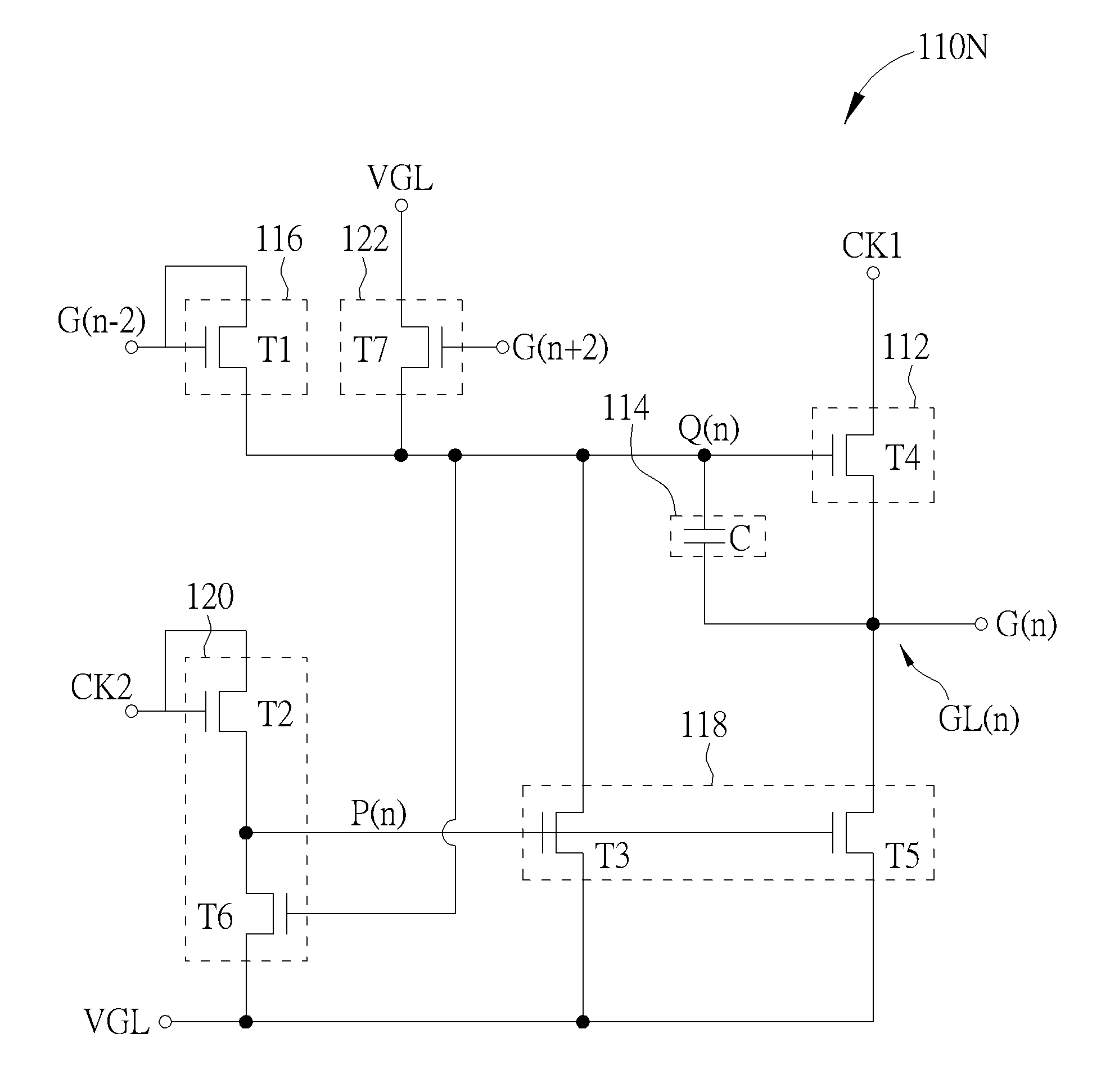
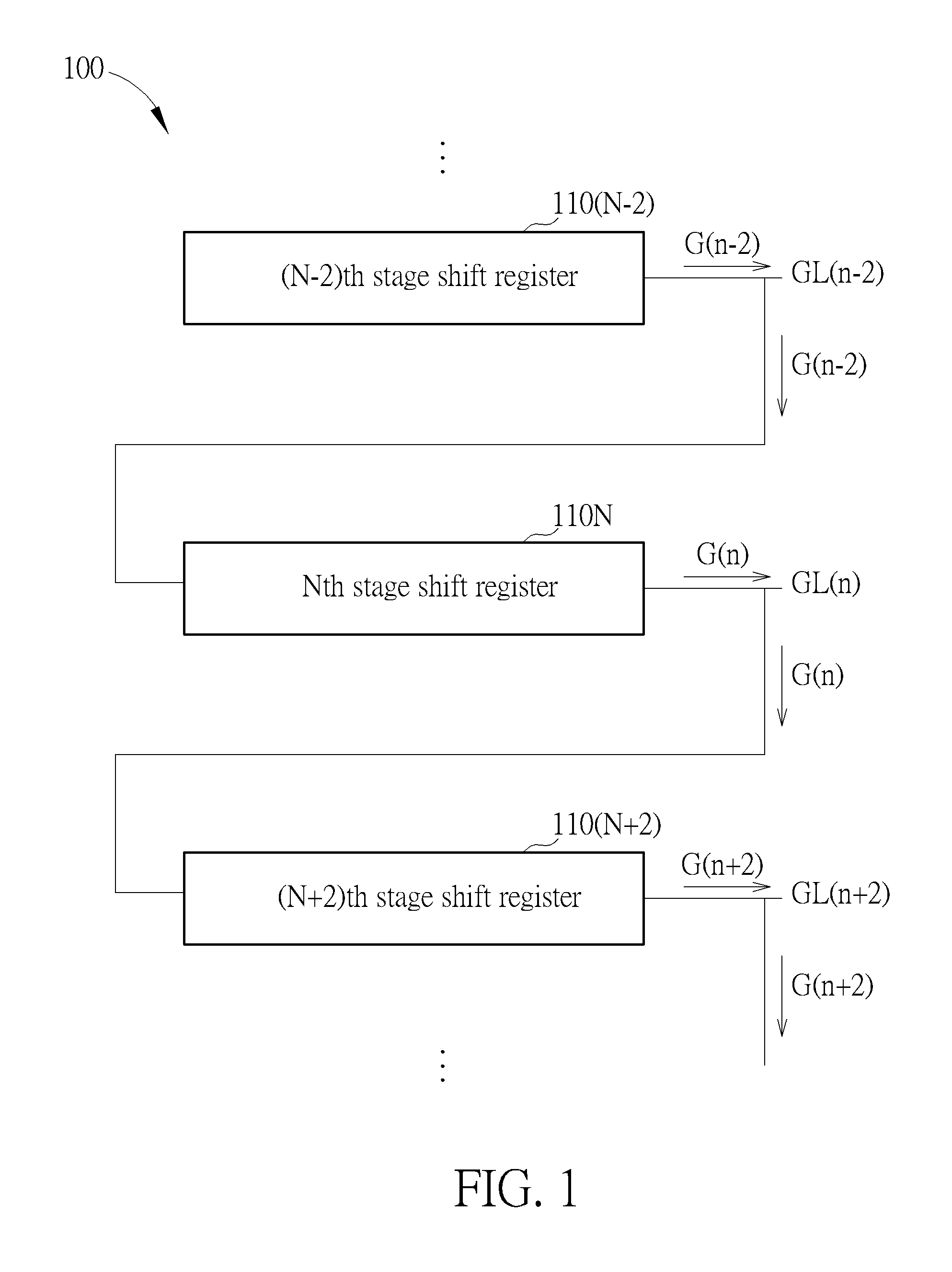
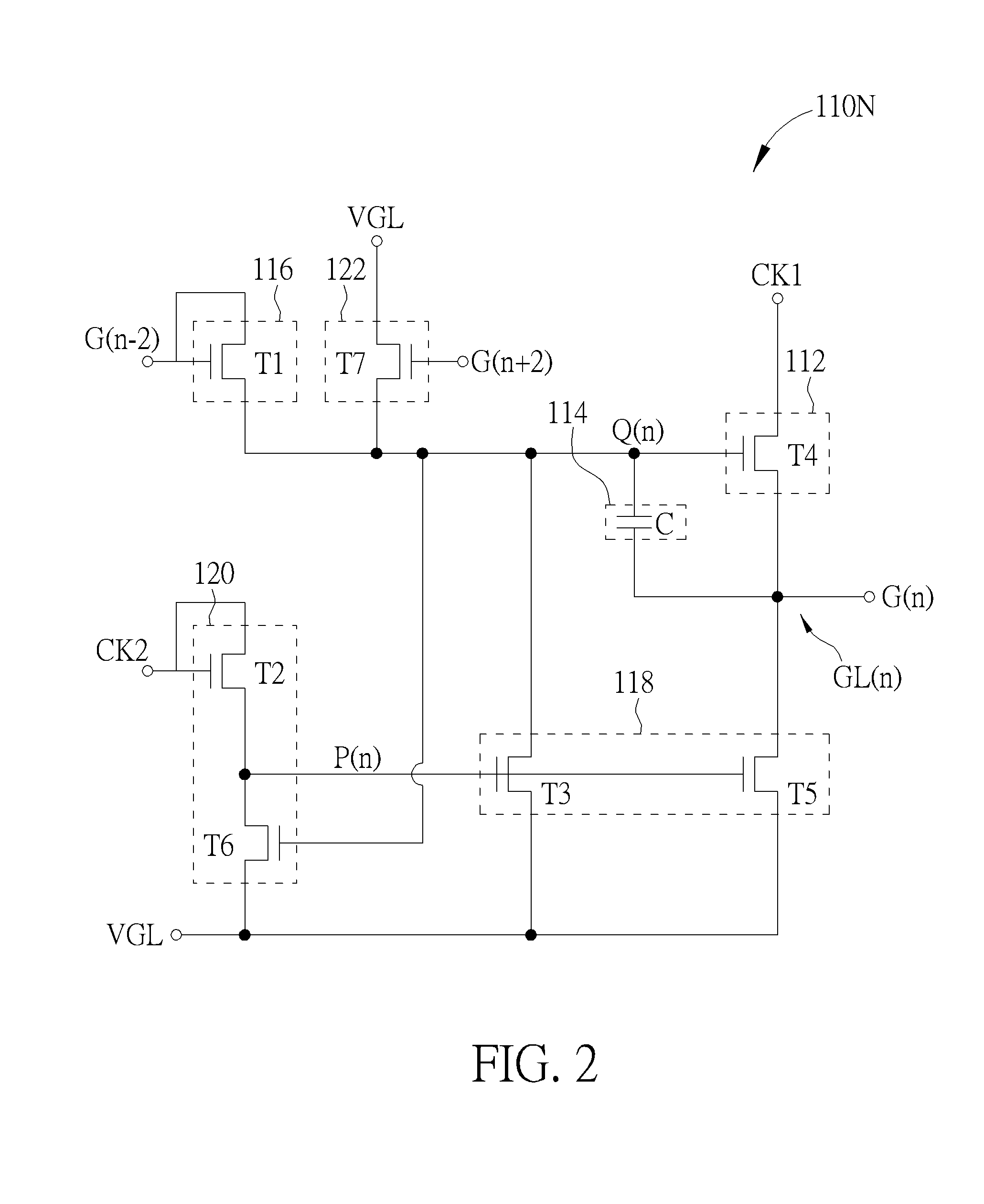
[0014]Please refer to FIG. 1 and FIG. 2. FIG. 1 is a diagram showing a gate driving circuit of the present invention. FIG. 2 is a diagram showing an Nth stage shift register of the gate driving circuit of FIG. 1. As shown in figures, the gate driving circuit 100 comprises plural-stage shift registers 110. For ease of explanation, the gate driving circuit only illustrates an (N−2) th stage shift register 110 (N−2), an Nth stage shift register 110N, and an (N+2)th stage shift register 110 (N+2), wherein only an internal structure of the Nth stage shift register 110N is illustrated in FIG. 2. The other shift registers are similar to the Nth stage shift register 110N, thus, no further illustration is provided. The (N−2) th stage shift register 110(N−2) is for outputting a (N−2) th stage gate signal G(n−2). The Nth stage shift register 110N is for outputting an Nth stage gate signal G(n). The (N+2) th stage shift register 110 (N+2) is for outputting a (N+2)th stage gate signal G(n+2). Th...
second embodiment
[0025]Please refer to FIG. 4, and refer to FIG. 1 and FIG. 2 as well. FIG. 4 is a diagram showing waveforms of related signals of the Nth stage shift register. As shown in FIG. 4, the first clock signal CK1 and the second clock signal CK2 have the same pulse width, and the rising edge of the first clock signal CK1 leads the rising edge of the second clock signal CK2 by ½ pulse width. Operations of the Nth stage shift register in FIG. 4 is similar to the above illustration, thus no further explanation is provided. In the embodiments of the present invention, the rising edge of the first clock signal CK1 leads the rising edge of the second clock signal CK2 by ¼ to ½ pulse width.
[0026]Please refer to FIG. 5. FIG. 5 is a diagram showing a second embodiment of the Nth stage shift register of the gate driving circuit of FIG. 1. Besides driving unit 116′ and auxiliary pull-down unit 122′ in FIG. 5, other components of the Nth stage shift register 110N′ are identical to the components of th...
third embodiment
[0027]Please refer to FIG. 6. FIG. 6 is a diagram showing the Nth stage shift register of the gate driving circuit of FIG. 1. Besides auxiliary pull-down unit 122″ in FIG. 6, other components of the Nth stage shift register 110N″ are identical to the components of the Nth stage shift register 110N in FIG. 2. The auxiliary pull-down unit 122″ comprises an auxiliary pull-down transistor T7. A first end of the auxiliary pull-down transistor T7 is configured to receive the (N−2)th stage gate signal G(n−2), a control end of the auxiliary pull-down transistor T7 is configured to receive the (N+2)th stage gate signal G(n+2) or a third clock signal CK3, and a second end of the auxiliary pull-down transistor T7 is electrically connected to the energy-store unit 114. A phase of the third clock signal CK3 is opposite to a phase of the first clock signal CK1. According to the above arrangement, when the auxiliary pull-down unit 122″ receives the (N+2) th stage gate signal G(n+2) pulled up to th...
PUM
 Abstract
Description
Claims
Application Information