Seamless gap-fill with spatial atomic layer deposition

a technology of atomic layer deposition and gap filling, applied in the field of substrate processing, can solve the problems of difficult to completely fill gaps and trenches in these structures without creating, too much electrical noise, and fabrication problems, and achieve the effect of high aspect ratio trenches and high aspect ratio features

Inactive Publication Date: 2015-09-10
APPLIED MATERIALS INC
View PDF3 Cites 247 Cited by
  • Summary
  • Abstract
  • Description
  • Claims
  • Application Information

AI Technical Summary

Problems solved by technology

While the ability to make device structures with ever increasing aspect ratios has allowed more structures (e.g., transistors, capacitors, diodes, etc.) to be packed onto the same surface area of a semiconductor chip substrate, it has also created fabrication problems.
One of these problems is the difficulty of completely filling the gaps and trenches in these structures without creating a void or seam during the filling process.
If the gaps were left empty, there would be too much electrical noise, and current leakage for the devices to operate properly (or at all).
As aspect ratios increased to 3:1 or above, however, it became more difficult to fill the deep, narrow trench without having a blockage start a void or seam in the fill volume.

Method used


Image

  • Seamless gap-fill with spatial atomic layer deposition
  • Seamless gap-fill with spatial atomic layer deposition
  • Seamless gap-fill with spatial atomic layer deposition

Examples


Embodiment Construction

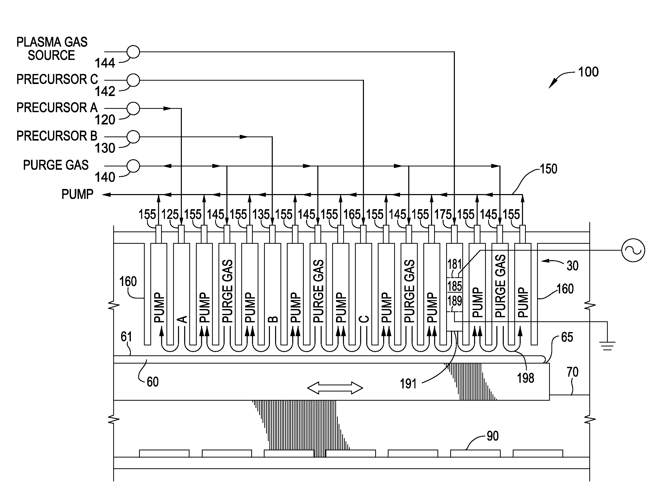
[0017]Embodiments disclosed herein generally relate to the processing of substrates, and more particularly, relate to methods for forming dielectric materials in high aspect ratio features. In one embodiment, a method for filling high aspect ratio trenches is disclosed. The method includes placing a substrate inside a processing chamber, where the substrate has a surface having a plurality of high aspect ratio trenches and the surface is facing a gas / plasma distribution assembly. The method further includes performing a sequence of depositing a layer of dielectric material on the surface of the substrate and inside each of the plurality of trenches, where the layer of dielectric material is on a bottom and side walls of each trench, and removing a portion of the layer of dielectric material disposed on the surface of the substrate, where an opening of each trench is widened. The method further includes repeating the sequence until the trenches are filled seamlessly with the dielectr...


PUM

PropertyMeasurementUnit
thicknessaaaaaaaaaa
thicknessaaaaaaaaaa
aspect ratioaaaaaaaaaa

Abstract

Embodiments disclosed herein generally relate to forming dielectric materials in high aspect ratio features. In one embodiment, a method for filling high aspect ratio trenches in one processing chamber is disclosed. The method includes placing a substrate inside a processing chamber, where the substrate has a surface having a plurality of high aspect ratio trenches and the surface is facing a gas / plasma distribution assembly. The method further includes performing a sequence of depositing a layer of dielectric material on the surface of the substrate and inside each of the plurality of trenches, where the layer of dielectric material is on a bottom and side walls of each trench, and removing a portion of the layer of dielectric material disposed on the surface of the substrate, where an opening of each trench is widened. The sequence repeats until the trenches are filled seamlessly with the dielectric material.

Description

CROSS-REFERENCE TO RELATED APPLICATIONS[0001]This application claims priority to U.S. Provisional Patent Application Ser. No. 61 / 948,940, filed on Mar. 6, 2014, which herein is incorporated by reference.[0002]BACKGROUND[0003]1. Field[0004]Embodiments disclosed herein generally relate to the processing of substrates, and more particularly, relate to methods for forming dielectric materials in high aspect ratio features.[0005]2. Description of the Related Art[0006]As the device density on integrated circuits continues to increase, the size and distance between device structures continue to decrease. The narrower widths in the gaps of the structures and the trenches between structures increase the ratio of height to width (i.e., the aspect ratio) in these formations. In other words, the continued miniaturization of integrated circuit elements is shrinking the horizontal width within and between these elements faster than their vertical height.[0007]While the ability to make device stru...

Claims


Application Information

Patent Timeline
Patent Type & Authority Applications(United States)
IPC IPC(8): H01L21/762H01L21/02H01L21/311
CPCH01L21/76224H01L21/02274H01L21/31116H01L21/02164H01L21/0217H01L21/0228C23C16/045C23C16/345C23C16/402C23C16/45551
Inventor LI, NINGNGUYEN, VICTORBALSEANU, MIHAELAXIA, LI-QUNMARCUS, STEVEN D.YANG, HAICHUNTANAKA, KEIICHI
Owner APPLIED MATERIALS INC
Why Eureka
Try Eureka