Method for Manufacturing Display Device and Method for Manufacturing Electronic Device

Active Publication Date: 2015-09-17
SEMICON ENERGY LAB CO LTD
View PDF7 Cites 31 Cited by
  • Summary
  • Abstract
  • Description
  • Claims
  • Application Information

AI Technical Summary

Benefits of technology

The technical effects of this patent are to provide a method for manufacturing a display device that does not easily damage the electrodes or display region, and maintains high reliability and manufacturing yield. Additionally, the method and display device provide high visibility, display quality, reliability, low power consumption, and are less likely to be broken.

Problems solved by technology

However, a method in which part of a flexible substrate is removed by a laser beam or with an edged tool has a problem in that an electrode included in a display device is damaged easily and the reliability and manufacturing yield of the display device are reduced easily.

Method used


Image

  • Method for Manufacturing Display Device and Method for Manufacturing Electronic Device
  • Method for Manufacturing Display Device and Method for Manufacturing Electronic Device
  • Method for Manufacturing Display Device and Method for Manufacturing Electronic Device

Examples


embodiment 1

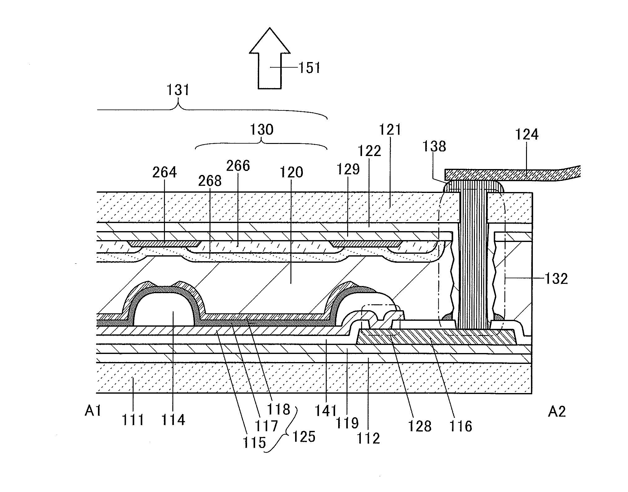
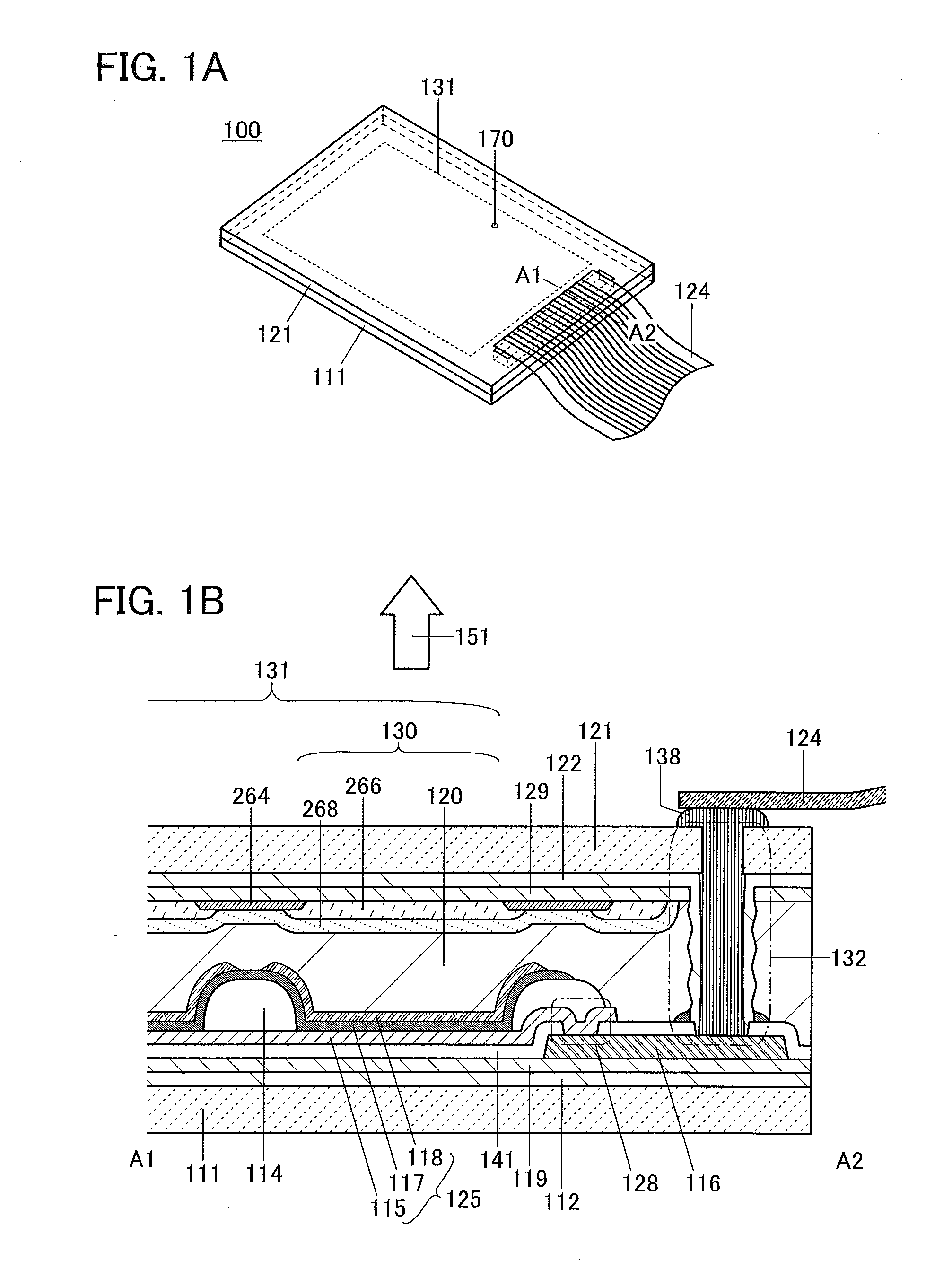
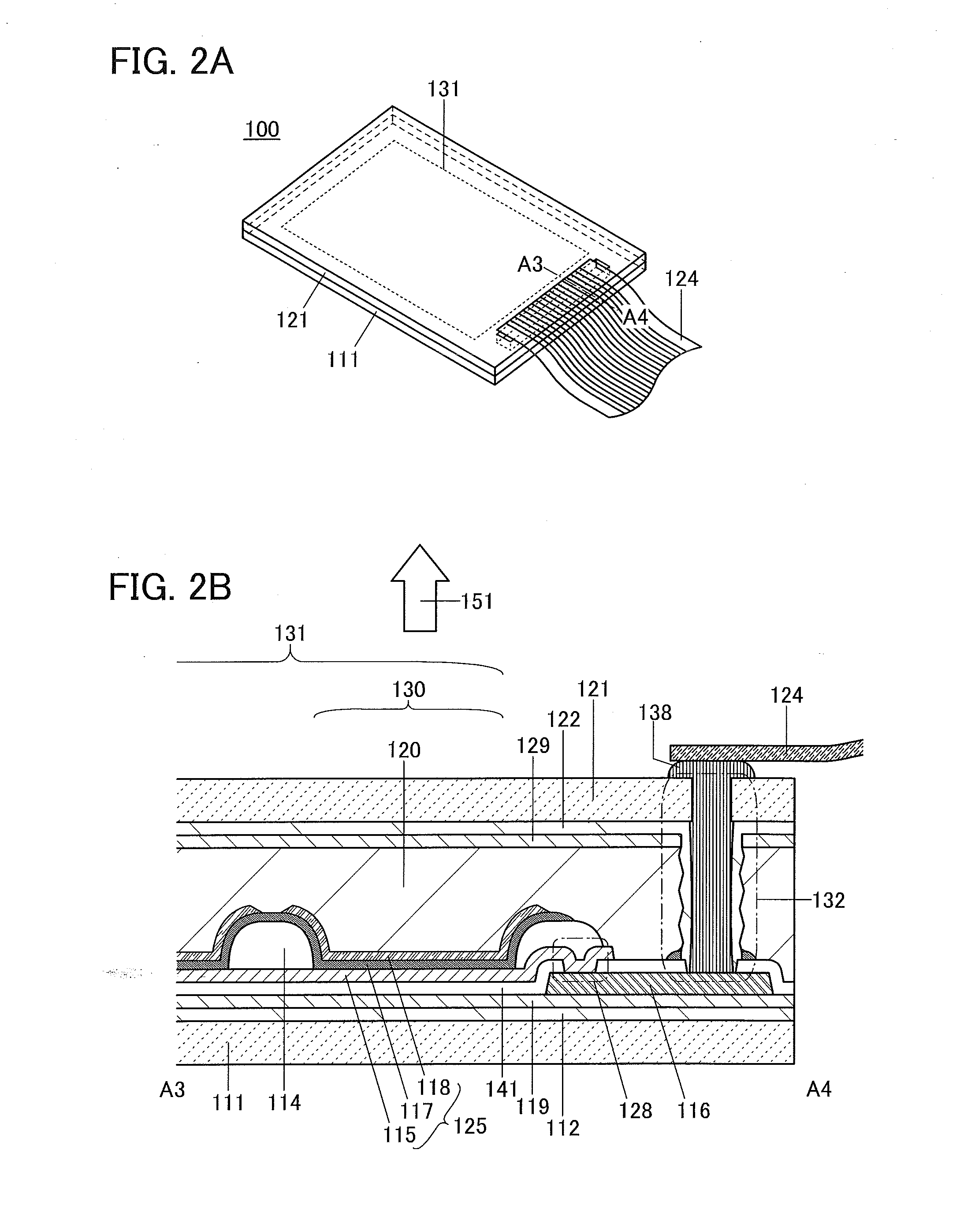
[0060]A structure example of a display device 100 of one embodiment of the present invention will be described with reference to FIGS. 1A and 1B, FIGS. 2A and 2B, FIGS. 3A and 3B, FIGS. 4A to 4E, FIGS. 5A to 5D, FIGS. 6A to 6F, FIGS. 7A to 7C, FIGS. 8A and 8B, FIGS. 9A and 9B, FIGS. 10A and 10B, FIGS. 11A and 11B, and FIGS. 12A and 12B. FIG. 1A is a perspective view of the display device 100 to which an external electrode 124 is connected, and FIG. 1B is a cross-sectional view taken along the dashed-dotted line A1-A2 in FIG. 1A. Note that the display device 100 disclosed in this specification is a display device in which a light-emitting element is used as a display element. As the display device 100 of one embodiment of the present invention, a display device having a top-emission structure is described as an example. Note that the display device 100 can be a display device having a bottom-emission structure or a dual-emission structure.

[0061]The display device 100 described in thi...

embodiment 2

[0154]In this embodiment, a display device 200 having a structure different from the structure of the display device 100 described in the above embodiment will be described with reference to FIGS. 14A and 14B. FIG. 14A is a perspective view of the display device 200, and FIG. 14B is a cross-sectional view taken along the dashed-dotted line A5-A6 in FIG. 14A.

[0155]The display device 200 described in this embodiment includes a display region 231 and a peripheral circuit 251. The display device 200 further includes the electrode 116 and the light-emitting element 125 including the electrode 115, the EL layer 117, and the electrode 118. A plurality of light-emitting elements 125 are formed in the display region 231. A transistor 232 for controlling the amount of light emitted from the light-emitting element 125 is connected to each light-emitting element 125.

[0156]The electrode 116 is electrically connected to the external electrode 124 through the anisotropic conductive connection laye...

embodiment 3

[0191]In this embodiment, a specific structure example of the display device 200 will be described with reference to FIGS. 17A to 17C. FIG. 17A is a block diagram illustrating the structure example of the display device 200.

[0192]The display device 200 illustrated in FIG. 17A includes the display region 231, a driver circuit 142a, a driver circuit 142b, and a driver circuit 133. The driver circuits 142a, 142b, and 133 collectively correspond to the peripheral circuit 251 described in the above embodiments. The driver circuits 142a, 142b, and 133 are collectively referred to as a driver circuit portion in some cases.

[0193]The driver circuits 142a and 142b function as, for example, scan line driver circuits. The driver circuit 133 functions as, for example, a signal line driver circuit. Note that one of the driver circuits 142a and 142b may be omitted. Alternatively, some sort of circuit facing the driver circuit 133 with the display region 231 provided therebetween may be provided.

[0...


PUM


Abstract

A method for manufacturing a display device is provided. The method includes: forming, between a first substrate and a second substrate, a light-emitting element including an electroluminescence layer and a wiring over which a peeling layer formed by using the material of the electroluminescence layer is provided; and peeling whole of the second substrate from the first substrate so that the peeling layer over the wiring is simultaneously exposed.

Description

BACKGROUND OF THE INVENTION[0001]1. Field of the Invention[0002]The present invention relates to a display device. The present invention also relates to a method for manufacturing the display device.[0003]Note that one embodiment of the present invention is not limited to the above technical field.[0004]Note that in this specification and the like, a semiconductor device generally means a device that can function by utilizing semiconductor characteristics. Thus, a semiconductor element such as a transistor or a diode and a semiconductor circuit are semiconductor devices. A display device, a light-emitting device, a lighting device, an electro-optical device, an electronic device, and the like may include a semiconductor element or a semiconductor circuit. Therefore, a display device, a light-emitting device, a lighting device, an electro-optical device, an electronic device, and the like include a semiconductor device in some cases.[0005]2. Description of the Related Art[0006]In rec...

Claims


Application Information

Patent Timeline
IPC IPC(8): H01L51/56H01L51/50H01L27/32H01L51/00
CPCH01L51/56H01L51/0097H01L51/5012H01L2227/326H01L27/3244H01L2251/5338H01L2227/323H01L51/003Y02E10/549Y02P70/50H10K59/12H10K59/131H10K71/80H10K77/111H10K50/11H10K59/1201H10K59/10H10K71/00H10K50/805
Inventor SAKUISHI, TATSUYANAKAMURA, DAIKICHIDA, AKIHIROAOYAMA, TOMOYA
Owner SEMICON ENERGY LAB CO LTD
Why Eureka
Try Eureka