
Method for forming a doped silicon ingot of uniform resistivity

a technology of uniform resistivity and silicon ingot, which is applied in the direction of control devices for lighting and heating apparatus, crystal growth process, furnaces, etc., can solve the problems of difficult to use the whole of a silicon ingot of variable resistivity, contaminating the silicon by other impurities, and tedious technique, etc., to achieve uniform electrical resistivity, simple and economical, good metallurgical quality

Inactive Publication Date: 2015-10-08
COMMISSARIAT A LENERGIE ATOMIQUE ET AUX ENERGIES ALTERNATIVES
View PDF2 Cites 5 Cited by
  • Summary
  • Abstract
  • Description
  • Claims
  • Application Information

AI Technical Summary

Benefits of technology

The patent text talks about a need for a simple and cost-effective way to make high-quality silicon ingots with uniform electrical resistivity. The technical effect of this invention is to provide such a method.

Problems solved by technology

It is however difficult to use the whole of a silicon ingot of variable resistivity.
This technique is tedious as it is necessary, at each addition step, to remove the ingot from the bath and wait until the dopants and the silicon have completely melted.
Under these conditions, addition of dopants is accompanied by a contamination of the silicon by other impurities, in particular metallic impurities, which are detrimental for photovoltaic applications.
However, doping by transmutation can only be performed in a nuclear reactor.
It is therefore not applicable on a large scale and at low cost.

Method used


Image

  • Method for forming a doped silicon ingot of uniform resistivity
  • Method for forming a doped silicon ingot of uniform resistivity
  • Method for forming a doped silicon ingot of uniform resistivity

Examples


Embodiment Construction

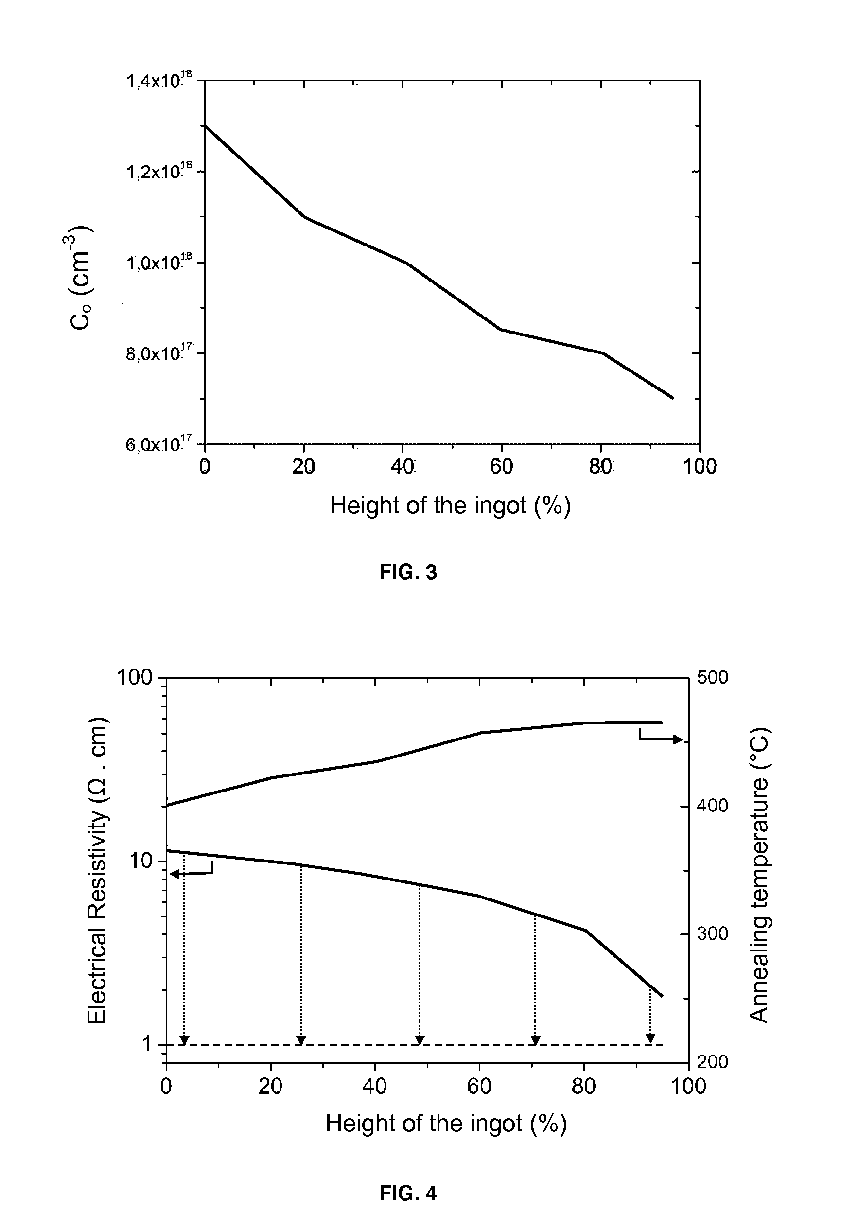
[0023]The technique proposed in the following consists in correcting the resistivity of a silicon ingot by locally forming thermal donors to tend towards an identical target resistivity in the whole ingot.

[0024]The single-crystal silicon obtained by the Czochralski method contains oxygen, typically between 1017 and 2×10¹⁸ atoms / cm3, and in particular interstitial oxygen (i.e. the oxygen atoms occupy interstitial positions in the crystal lattice).

[0025]At a temperature comprised between 350° C. and 550° C., the interstitial oxygen does however form clusters called Double Thermal Donors (DDT). Each thermal donor DDT generates two free electrons, which results in a variation of the electrical resistivity.

[0026]The electrical resistivity ρ does in fact vary according to two parameters, the concentration of majority free charge carriers and the mobility μ of these carriers, which depend on the concentration of double thermal donors NDDT. Its general expression is the following:

ρ(NDDT)=1m...


PUM

PropertyMeasurementUnit
Temperatureaaaaaaaaaa

Abstract

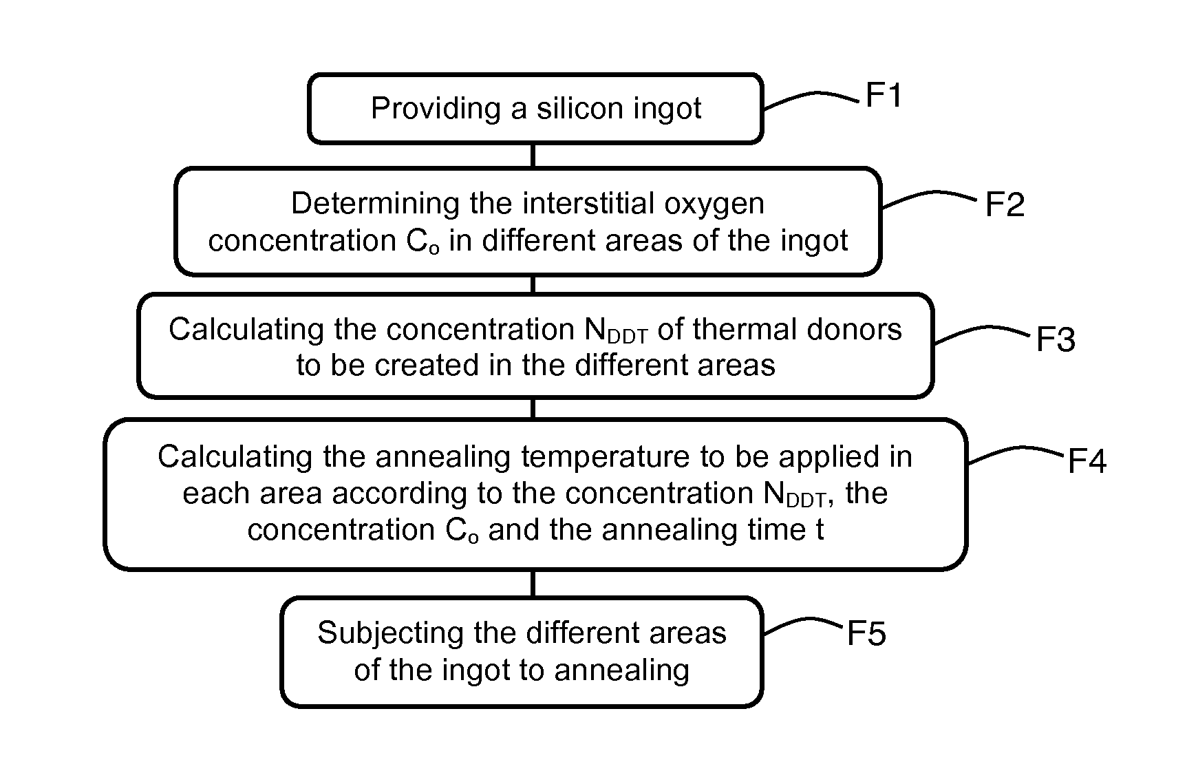
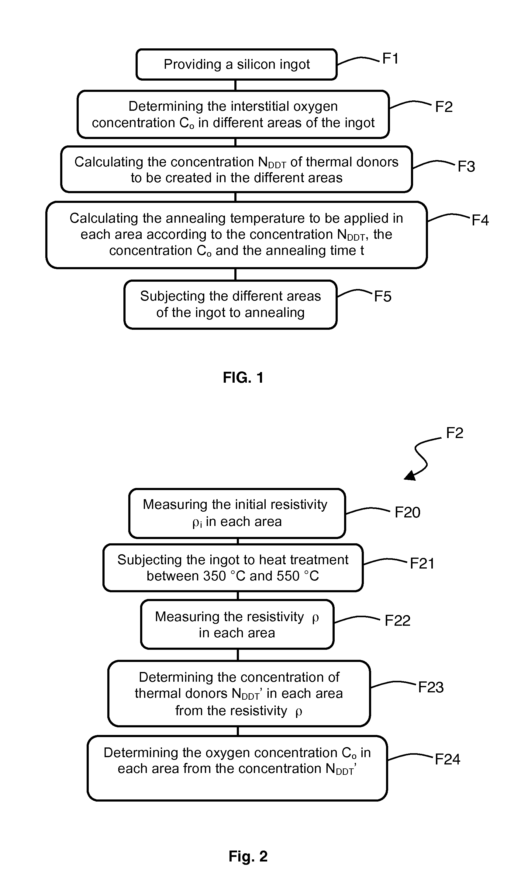
A method for forming a silicon ingot includes the following steps: providing a silicon ingot of variable electrical resistivity and containing interstitial oxygen, determining the interstitial oxygen concentration in different areas of the silicon ingot, calculating the concentration of thermal donors to be created in the different areas to reach a target value of the electrical resistivity, and subjecting the different areas of the silicon ingot to annealing so as to form the thermal donors. The annealing temperature in each area is determined from the thermal donor and interstitial oxygen concentrations of the area and from a predefined annealing time.

Description

BACKGROUND OF THE INVENTION[0001]The invention relates to a method for forming a silicon ingot, and more particularly a silicon ingot having a uniform resistivity.STATE OF THE ART[0002]The Czochralski method is a technique that is commonly used to form single-crystal silicon ingots. It consists in melting a quantity of silicon, called feedstock, in a crucible and in resolidifying the silicon from a seed. The seed, oriented with respect to a crystal axis of the solid silicon, is first dipped in the molten silicon bath. It is then drawn slowly upwards. The solid silicon ingot thus grows progressively feeding on the liquid bath.[0003]The silicon is generally doped to reduce its electrical resistivity. The dopants, such as boron and phosphorus, are incorporated before crystallization, either in the molten feedstock or in the feedstock before the melting step.[0004]With the Czochralski pulling method, the dopants tend to accumulate in the molten silicon bath on account of the segregation...

Claims


Application Information

Patent Timeline
IPC IPC(8): C30B33/02F27D19/00F27D21/00C30B29/06
CPCC30B33/02F27D21/00F27D19/00C30B29/06B28D1/22B28D5/0011G01N27/041
Inventor VEIRMAN, JORDIDUBOIS, SEBASTIENENJALBERT, NICOLAS
Owner COMMISSARIAT A LENERGIE ATOMIQUE ET AUX ENERGIES ALTERNATIVES
Learn More