
Multiple layer charge-coupled photovoltaic device

a photovoltaic device and charge-coupling technology, applied in the direction of basic electric elements, semiconductor devices, electrical equipment, etc., can solve the problems of low power and low efficiency of solar power, and achieve the effect of high power and high efficiency

Active Publication Date: 2015-10-22
ALLEN AARON RICHARD
View PDF3 Cites 4 Cited by
  • Summary
  • Abstract
  • Description
  • Claims
  • Application Information

AI Technical Summary

Benefits of technology

The present invention has several advantages, including the ability to convert wavelengths, trap light, capture and multiply photons, and store and output electron energy. It can be used in any light environment, is scalable, powerful, and efficient. The unique feature is that it integrates both gain and energy storage elements, specifically for solar energy purposes.

Problems solved by technology

Currently solar power suffers from low efficiencies and low powers.

Method used


Image

  • Multiple layer charge-coupled photovoltaic device
  • Multiple layer charge-coupled photovoltaic device
  • Multiple layer charge-coupled photovoltaic device

Examples


Embodiment Construction

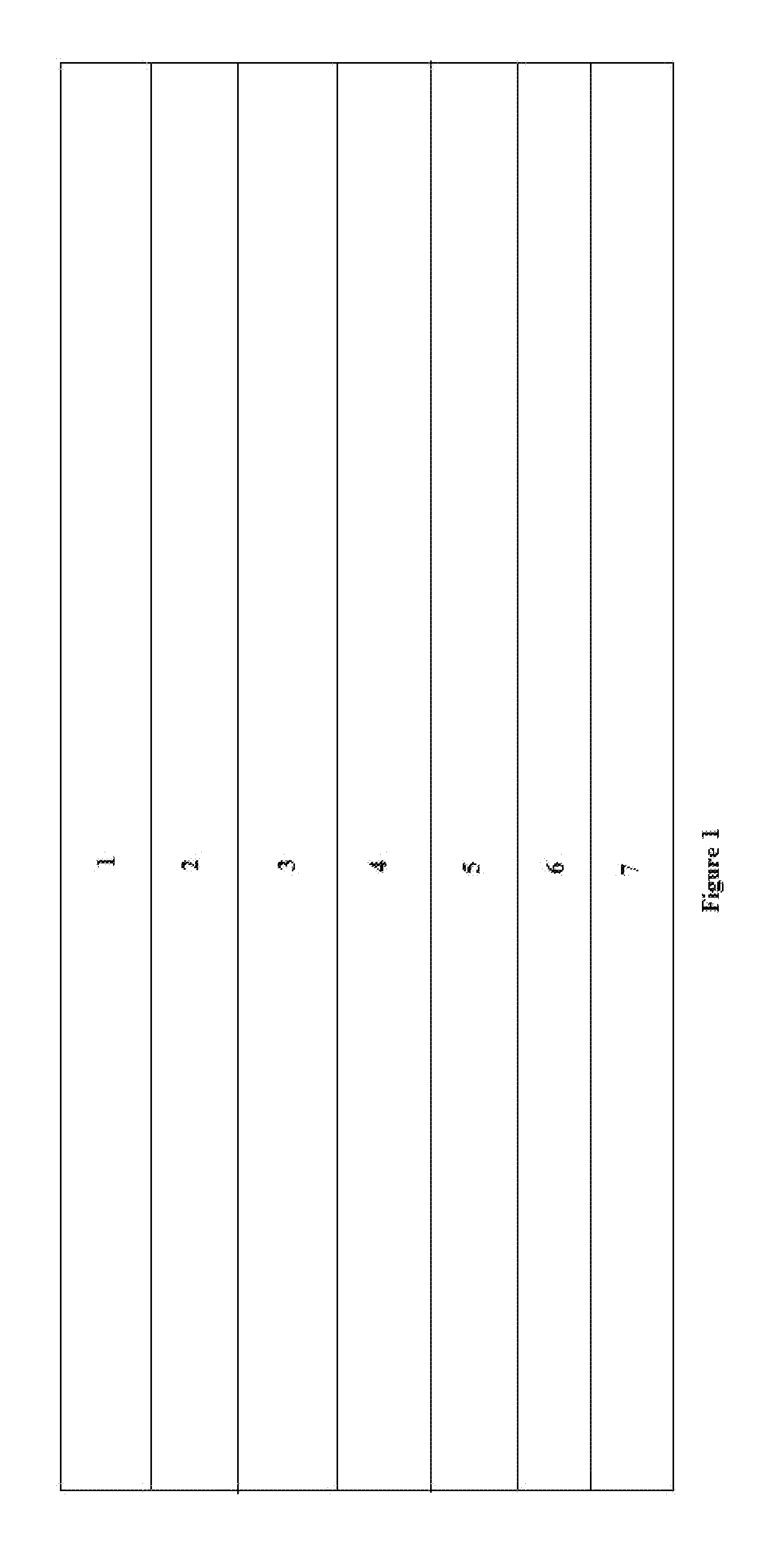
[0016]This description details a structure composed of multiple layers that consist of seven stages of photon and electron management, enhancement, and conversion for the purposes of photovoltaic applications. The invention consists of one or more layers comprised of: 1) an energy dependent up and down conversion layer optimized for a particular wavelength such as infrared; 2) a layer for multiple implementations of light capturing and trapping; 3) a layer for photonic and plasmonic enhancement of captured and trapped light; 4) a layer for converting photons to electrons; 5) a layer for multiplying electrons; 6) a layer for storing generated electrons; and 7) a layer for using electrons for power. One or more layers may serve simultaneous purposes.

[0017]This invention utilizes charge coupling and its high quantum efficiencies for solar energy. Once a charge buildup is initiated, the device will run at full power through series, parallel, or other scaling architecture to provide cons...


PUM


Abstract

A structure composed of multiple layers that consist of 7 stages of photon and electron management, enhancement, and conversion for the purposes of photovoltaic applications is described. The invention consists of one or more layers comprised of: 1) an energy dependent up and down conversion layer optimized for a particular wavelength such as infrared; 2) a layer for multiple implementations of light capturing and trapping; 3) a layer for photonic and plasmonic enhancement of captured and trapped light; 4) a layer for converting photons to electrons; 5) a layer for multiplying electrons; 6) a layer for storing generated electrons; and 7) a layer for using electrons for power. One or more layers may serve simultaneous purposes.

Description

CROSS REFERENCE TO RELATED APPLICATIONS[0001]Reference is made to commonly assigned, U.S. Provisional Patent Application Ser. No. 61 / 995831 by Allen, filed Apr. 21, 2014 and entitled “MULTIPLE LAYER CHARGE-COUPLED PHOTOVOLTAIC DEVICE”, the disclosure of which is incorporated herein by reference.FIELD OF THE INVENTION[0002]The present invention relates in general to both systems and processes for converting light into useable power. In particular, it relates to devices utilizing the photovoltaic, plasmonic, photonic bandgap, up conversion, down conversion, optical resonance, multiple carrier generation, quantum well storage, and charge-coupling processes to produce useable electric power.BACKGROUND OF THE INVENTION[0003]The purpose of this invention is to provide readily available solar power day or night at high efficiencies and high powers. Currently solar power suffers from low efficiencies and low powers. Solar energy is increasingly becoming a viable option for useable power. Th...

Claims


Application Information

Patent Timeline
Patent Type & Authority Applications(United States)
IPC IPC(8): H01L31/055H01L31/0352H01L31/053
CPCH01L31/055H01L31/035272H01L31/053H01L31/054Y02E10/52H10K30/87
Inventor ALLEN, AARON RICHARD
Owner ALLEN AARON RICHARD
Learn More