Memory architecture dividing memory cell array into independent memory banks

a memory cell array and memory technology, applied in the memory field, can solve the problems of increasing the area and cost of memory dies, affecting the transfer time greatly affects the random access cycle time of the dram, so as to achieve high bandwidth data access and high speed random access.

Active Publication Date: 2015-11-19
PIECEMAKERS TECH
View PDF9 Cites 1 Cited by
  • Summary
  • Abstract
  • Description
  • Claims
  • Application Information

AI Technical Summary

Benefits of technology

[0006]It is therefore one objective of the present invention to provide a circuit architecture and a latch-type local wordline drive circuit so that memories can share a global word line decoding circuit, thus greatly reducing influence of memory die areas to realize an architecture having multiple independent sets of memory banks.
[0009]The proposed memory architecture may provide a plurality of memory banks (a single memory cell array can include a plurality of memory banks) and implement seamless read / write operations by employing a latch-type wordline drive circuit, thereby achieving high bandwidth data access and high speed random access.

Problems solved by technology

However, the row transition time greatly affects random access cycle time of the DRAM.
However, as different banks need respective word line decoding circuits and respective control circuits, the architecture having multiple sets of banks causes increased areas and costs of memory dies.

Method used


Image

  • Memory architecture dividing memory cell array into independent memory banks
  • Memory architecture dividing memory cell array into independent memory banks
  • Memory architecture dividing memory cell array into independent memory banks

Examples


Embodiment Construction

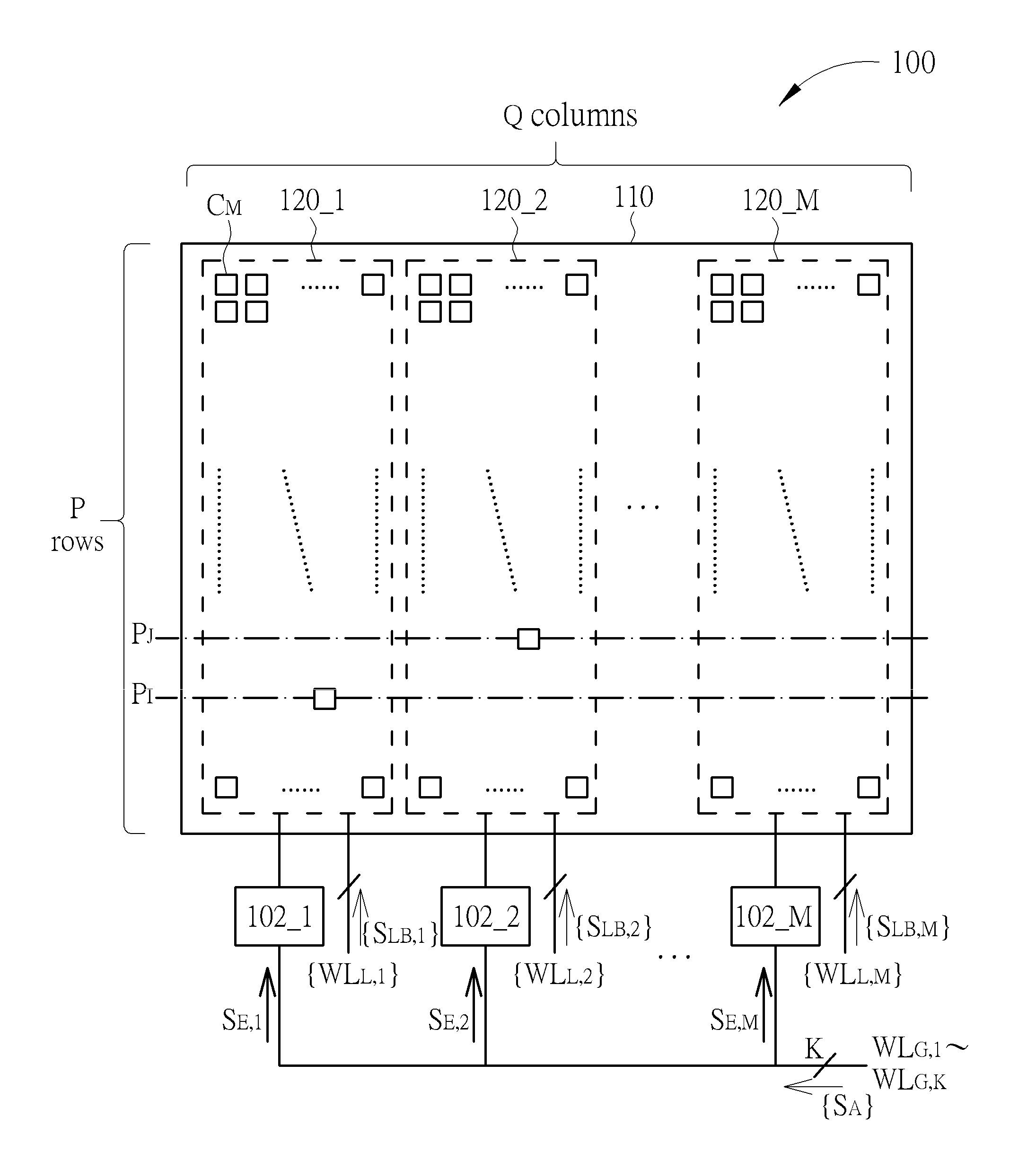
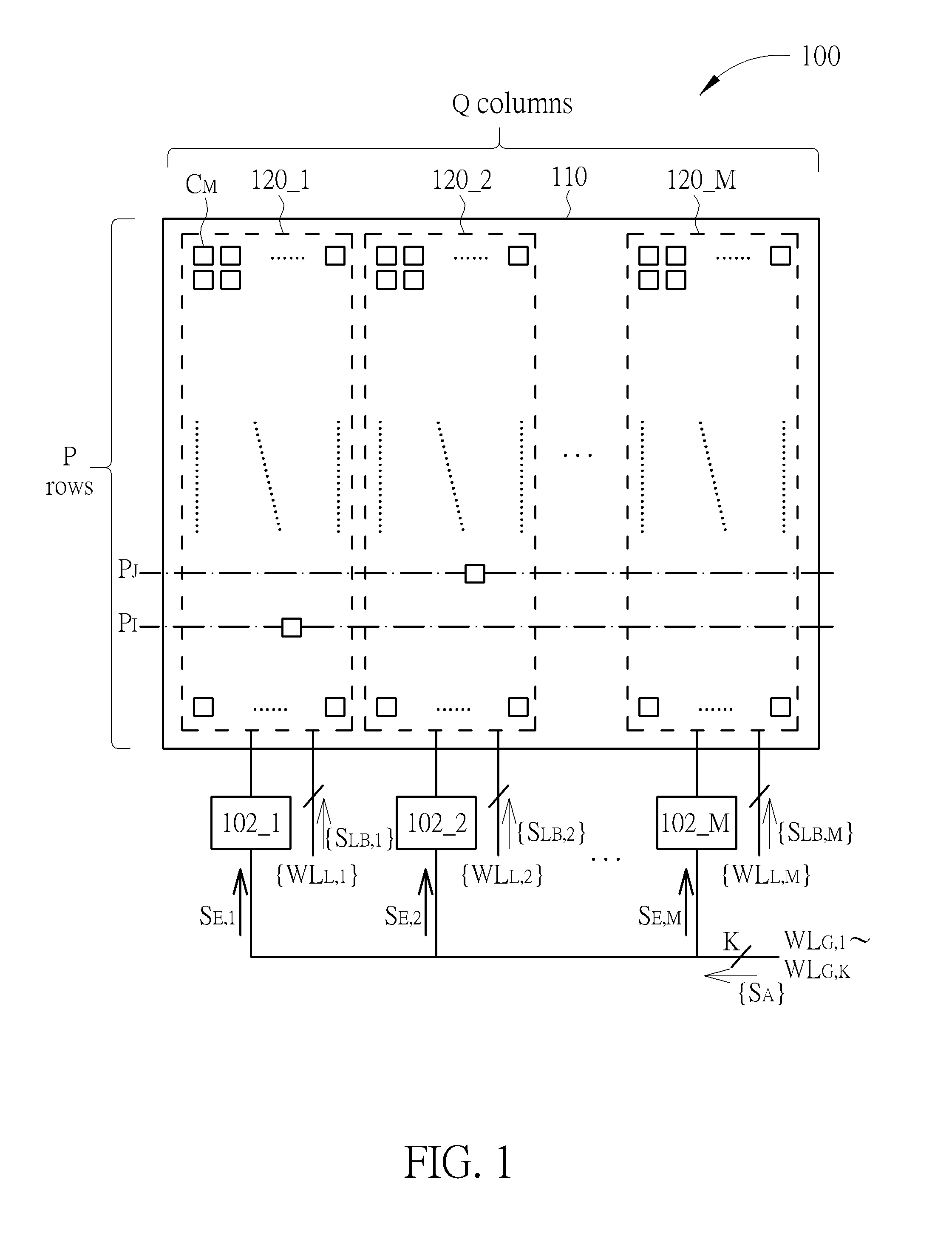
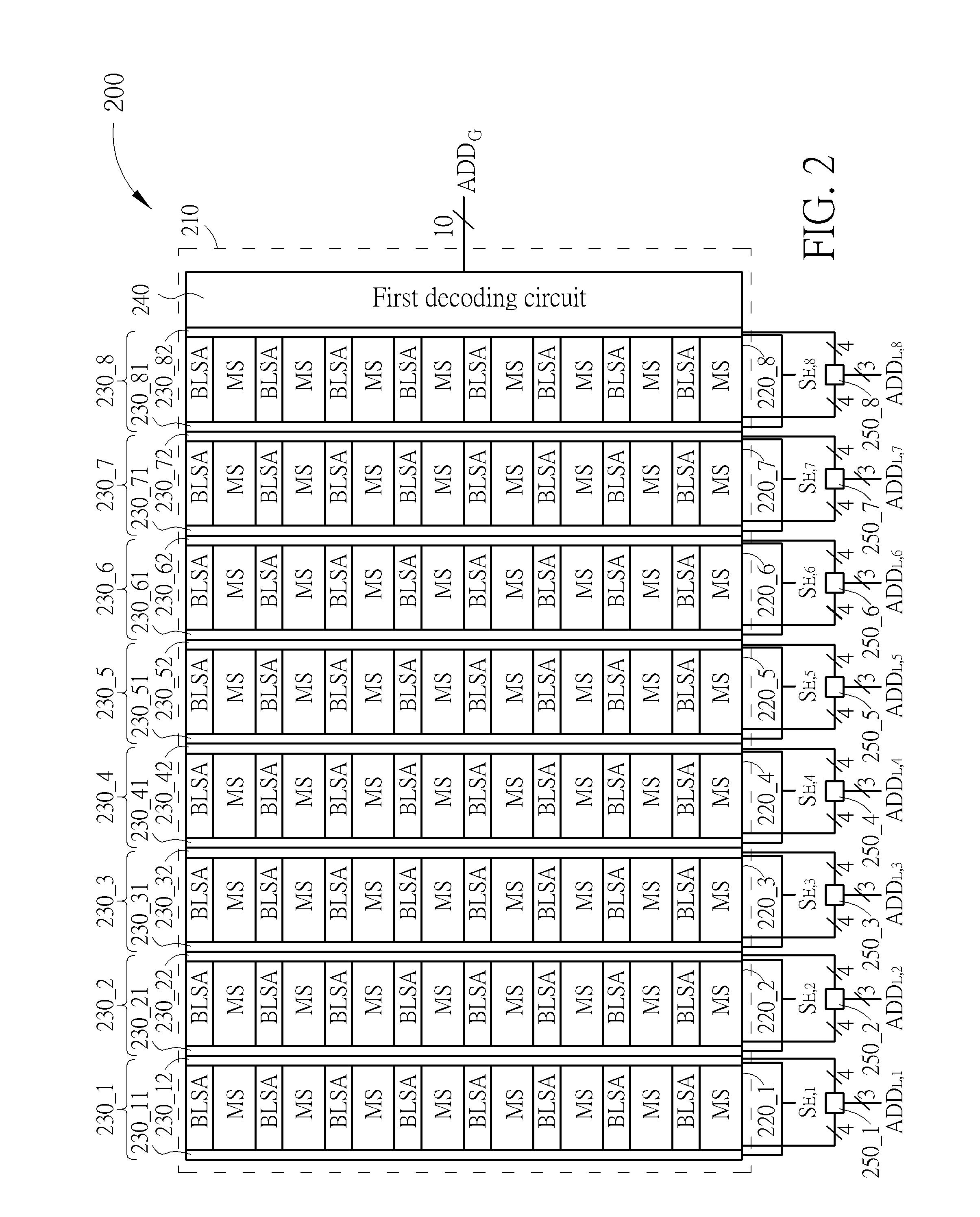
[0017]By dividing a memory cell array into a plurality of memory banks, which operate independently of each other, and employing a hierarchical wordline structure, the proposed memory architecture may provide high speed and flexible data access mechanism. Further description is provided below.

[0018]Please refer to FIG. 1, which is a diagram illustrating an exemplary memory architecture according to an embodiment of the present invention. The memory architecture 100 may include, but is not limited to, a memory cell array 110 which includes a plurality of memory cells arranged in P rows and Q columns (P and Q are positive integers), wherein each memory cell is labeled CM. Each memory cell may be disposed in correspondence with an intersection of a row and a column. By way of example but not limitation, each memory cell may be a one-transistor one-capacitor (1T1C) memory cell. The memory cell array 110 may further include M memory banks 120_1-120_M (M is a positive integer), wherein ea...


PUM


Abstract

A memory architecture includes K first wordlines, M groups of second wordlines, a memory cell array and M switch circuits. K and M are positive integers. Each group of second wordlines includes a plurality of second wordlines. The memory cell array includes M memory banks. The M memory banks are coupled to the M groups of second wordlines respectively, and receive independent M sets of second wordline signals through the M groups of second wordlines respectively. M switch circuits are disposed in correspondence with the M memory banks respectively. Each switch circuit selectively couples the K first wordlines to a corresponding memory bank so that the corresponding memory bank receives a shared set of first wordline signals through the K first wordline. Each memory bank performs a data access operation according to the received set of first wordline signals and a corresponding set of second wordline signals.

Description

BACKGROUND OF THE INVENTION[0001]1. Field of the Invention[0002]The disclosed embodiments of the present invention relate to memory, and more particularly, to a memory architecture which divides a memory cell array into a plurality of memory banks operating independently of each other.[0003]2. Description of the Prior Art[0004]In order to implement a layout of high density memory cells, a dynamic random access memory (DRAM) needs sufficient row transition time (row cycle time (tRC), which is usually longer than 30 ns). However, the row transition time greatly affects random access cycle time of the DRAM.[0005]One conventional method is to employ an architecture having multiple sets of banks, wherein the architecture can select respective word lines of different banks in parallel and access data of different banks in sequence. However, as different banks need respective word line decoding circuits and respective control circuits, the architecture having multiple sets of banks causes ...

Claims


Application Information

Patent Timeline
Patent Type & Authority Applications(United States)
IPC IPC(8): G11C11/408
CPCG11C11/4085G11C5/025G11C8/10G11C8/12G11C11/4087
Inventor TING, TAH-KANG JOSEPHWANG, GYH-BIN
Owner PIECEMAKERS TECH
Why Eureka
Try Eureka