Semiconductor device

Active Publication Date: 2015-11-26
RENESAS ELECTRONICS CORP
View PDF5 Cites 3 Cited by
  • Summary
  • Abstract
  • Description
  • Claims
  • Application Information

AI Technical Summary

Benefits of technology

[0006]According to one embodiment, an intermediate mode is set between an active mode in which the threshold voltage of a field-effect transistor is low and a standby mode in which the threshold voltage of the field-effect transistor is high. When a mode is shifted from the active mode to the standby mode, the threshold voltage for the active mode is raised temporarily to a threshold voltage for the intermediate

Problems solved by technology

However, when the active mode and the standby mode are switched

Method used


Image

  • Semiconductor device
  • Semiconductor device
  • Semiconductor device

Examples


Example

First Embodiment

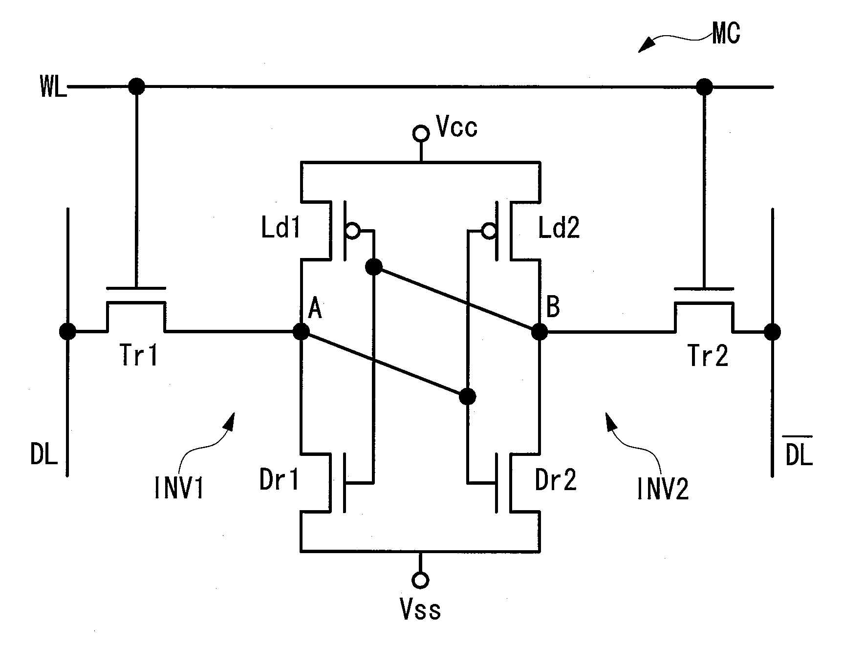
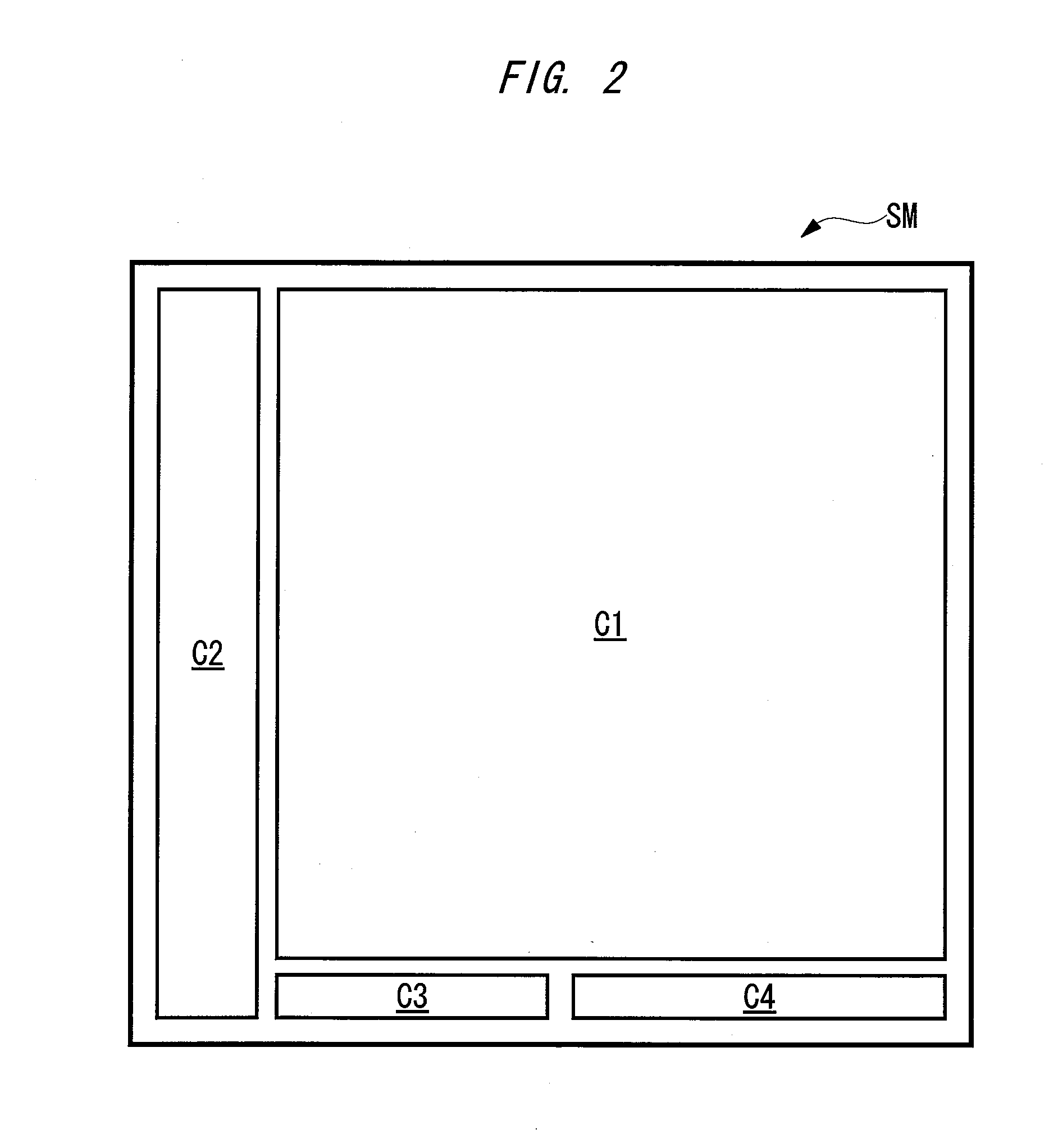
[0026]FIG. 2 is an internal configuration diagram of a semiconductor device according to a first embodiment.

[0027]A semiconductor device SM includes a plurality of circuits, such as a memory circuit C1, a control circuit C2, a substrate bias generating circuit C3, and a substrate bias timing control circuit C4. The memory circuit C1 stores therein data and programs, and the control circuit C2 calculates or controls data. Data and programs are thus exchanged between the memory circuit C1 and the control circuit C2.

[0028]When an external signal for shifting a mode from the active mode to the standby mode or from the standby mode to the active mode is input to the semiconductor device SM, the substrate bias generating circuit C3 generates a plurality of substrate biases different from each other. A substrate bias selected out of these a plurality of substrate biases by the substrate bias timing control circuit C4 is applied to memory cells of a plurality of SRAMs formed...

Example

Second Embodiment

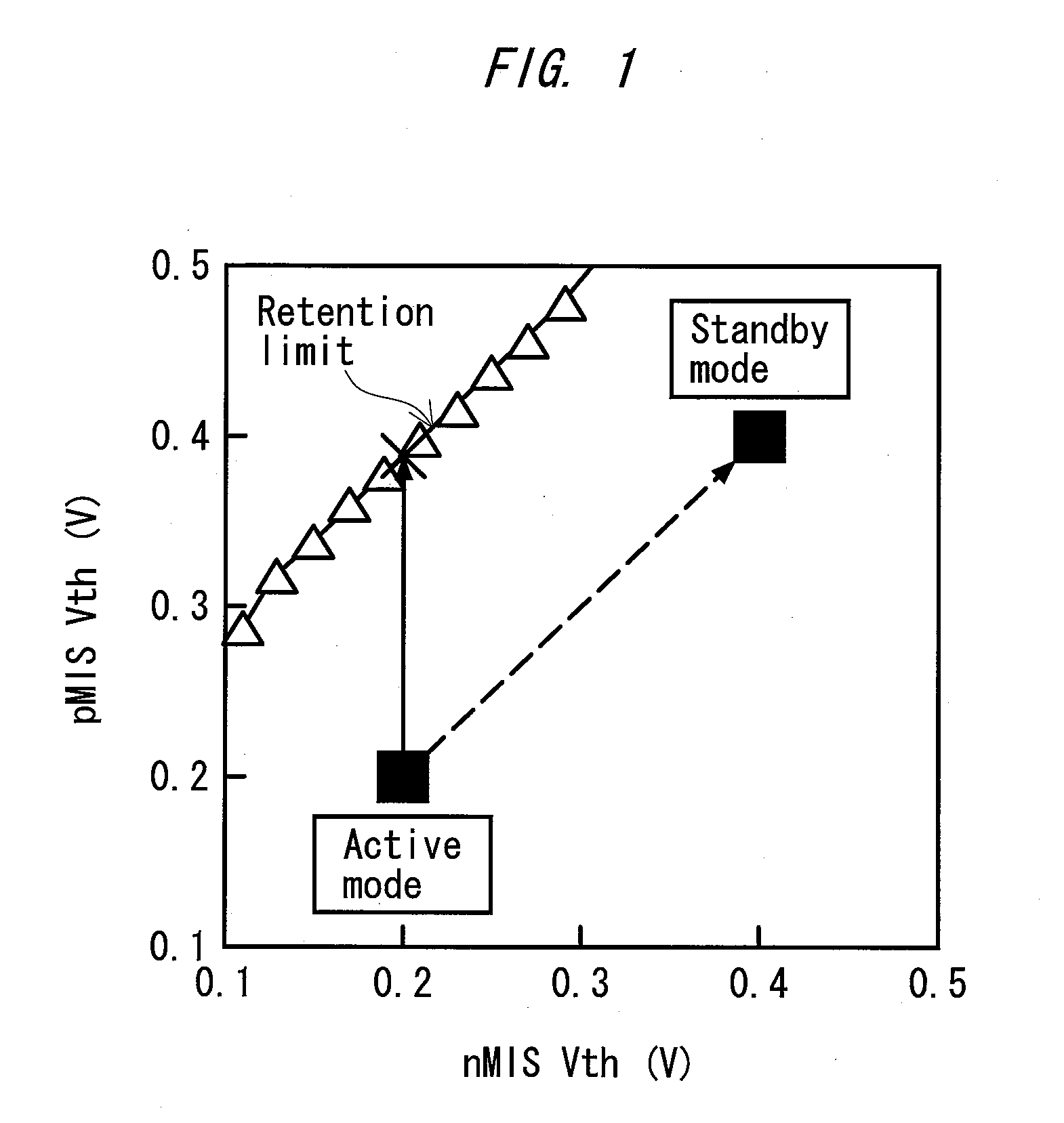
[0066]As shown in FIG. 1, a simulation result has clearly demonstrated that, in particularly, when a mode is shifted from the active mode in which the threshold voltage is low to the standby mode in which the threshold voltage is high, the threshold voltage of only the pMIS transistor rises transiently to exceed the data retention limit, thereby making data retention impossible. This possibly leads to a conclusion that when a mode is shifted from the active mode to the standby mode, data destruction is prevented by raising the threshold voltage of the nMIS transistor first, and that when a mode is shifted from the standby mode to the active mode, data destruction is prevented by lowering the threshold voltage of the pMIS transistor first.

[0067]A method of switching between the active mode and the standby mode according to a second embodiment will hereinafter be described.

[0068]FIG. 8 is a graph of an example of images of the balance of the threshold voltage of the p...


PUM


Abstract

An intermediate mode is set between the active mode in which a threshold voltage is low and a standby mode in which a threshold voltage is high. When a mode is shifted from the active mode to the standby mode, the threshold voltage for the active mode is raised temporarily to a threshold voltage for the intermediate mode and then the threshold voltage for the intermediate mode is raised to the threshold voltage for the standby mode. When a mode is shifted from the standby mode to the active mode, the threshold voltage for the standby mode is lowered temporarily to the threshold voltage for the intermediate mode and then the threshold voltage for the intermediate mode is lowered to the threshold voltage for the active mode.

Description

CROSS-REFERENCE TO RELATED APPLICATION[0001]The present application claims priority from Japanese Patent Application No. 2014-105855 filed on May 22, 2014, the content of which is hereby incorporated by reference into this application.TECHNICAL FIELD OF THE INVENTION[0002]The present invention relates to a semiconductor device, and to a technique that can be used preferably to a semiconductor device having a built-in SRAM (Static Random Access Memory) manufactured by, for example, an SOI (Silicon On Insulator) process.BACKGROUND OF THE INVENTION[0003]Japanese Laid-Open Patent Publication No. 2009-135140 (patent document 1) describes a semiconductor device having, for example, a thin-film BOX (Buried Oxide)-SOI structure and capable of achieving the high-speed operation of a logic circuit as well as the stable operation of a memory circuit. According to this semiconductor device, at least three or more well regions different in conductive property are formed in a semiconductor substr...

Claims


Application Information

Patent Timeline
IPC IPC(8): G11C11/419
CPCG11C11/419G11C11/413H01L27/1203H01L21/84G11C2207/2227H10B10/125G11C5/025G11C5/04G11C5/063G11C7/18G11C11/4097
Inventor YAMAMOTO, YOSHIKI
Owner RENESAS ELECTRONICS CORP
Why Eureka
Try Eureka