Organic insulator composition comprising high dielectric constant insulator dispersed in hyperbranched polymer and organic thin film transistor using the same
- Summary
- Abstract
- Description
- Claims
- Application Information
AI Technical Summary
Benefits of technology
Problems solved by technology
Method used
Image

Examples
example 1
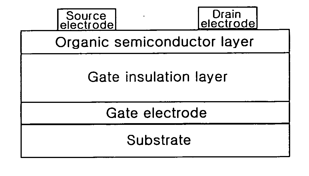
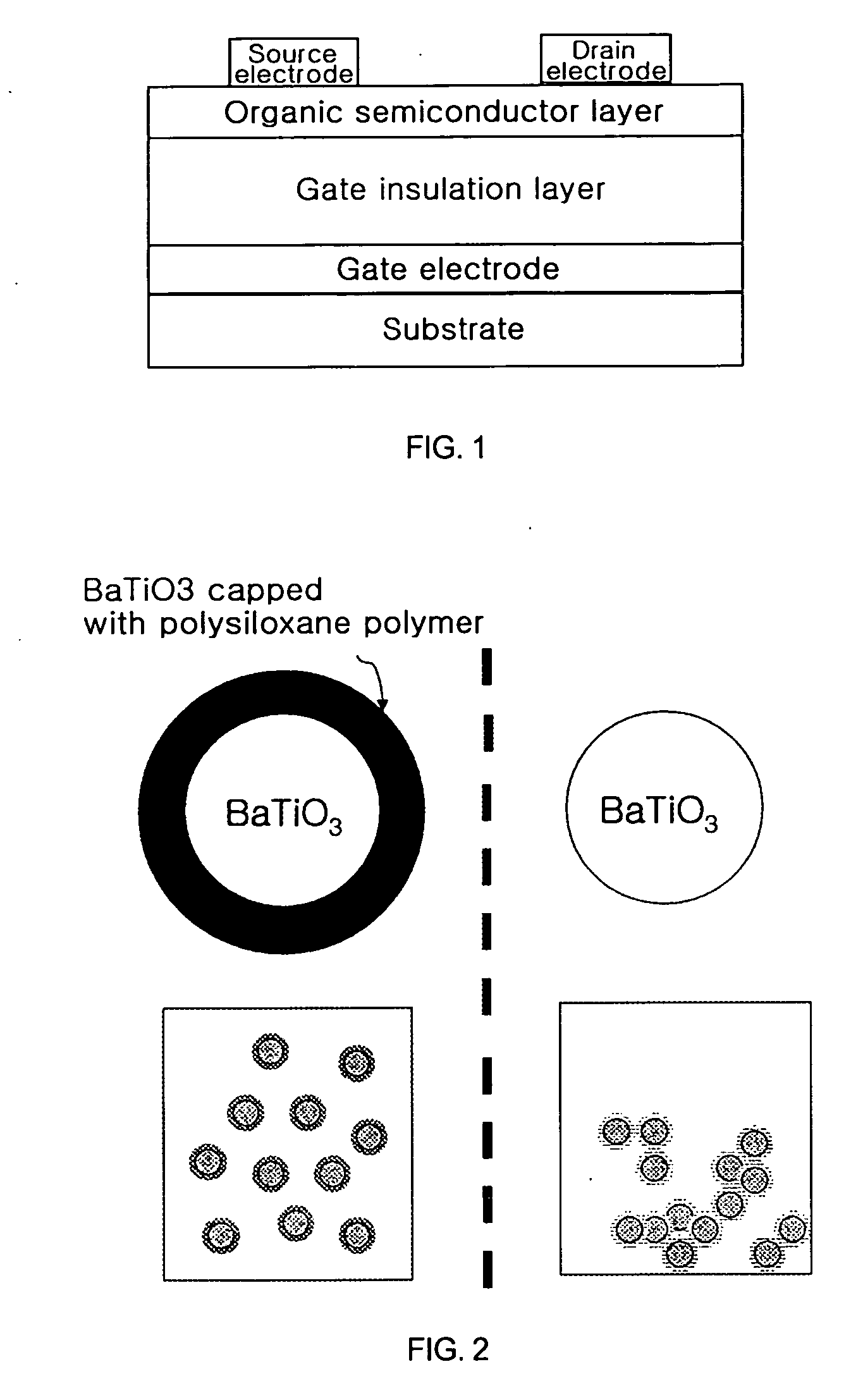
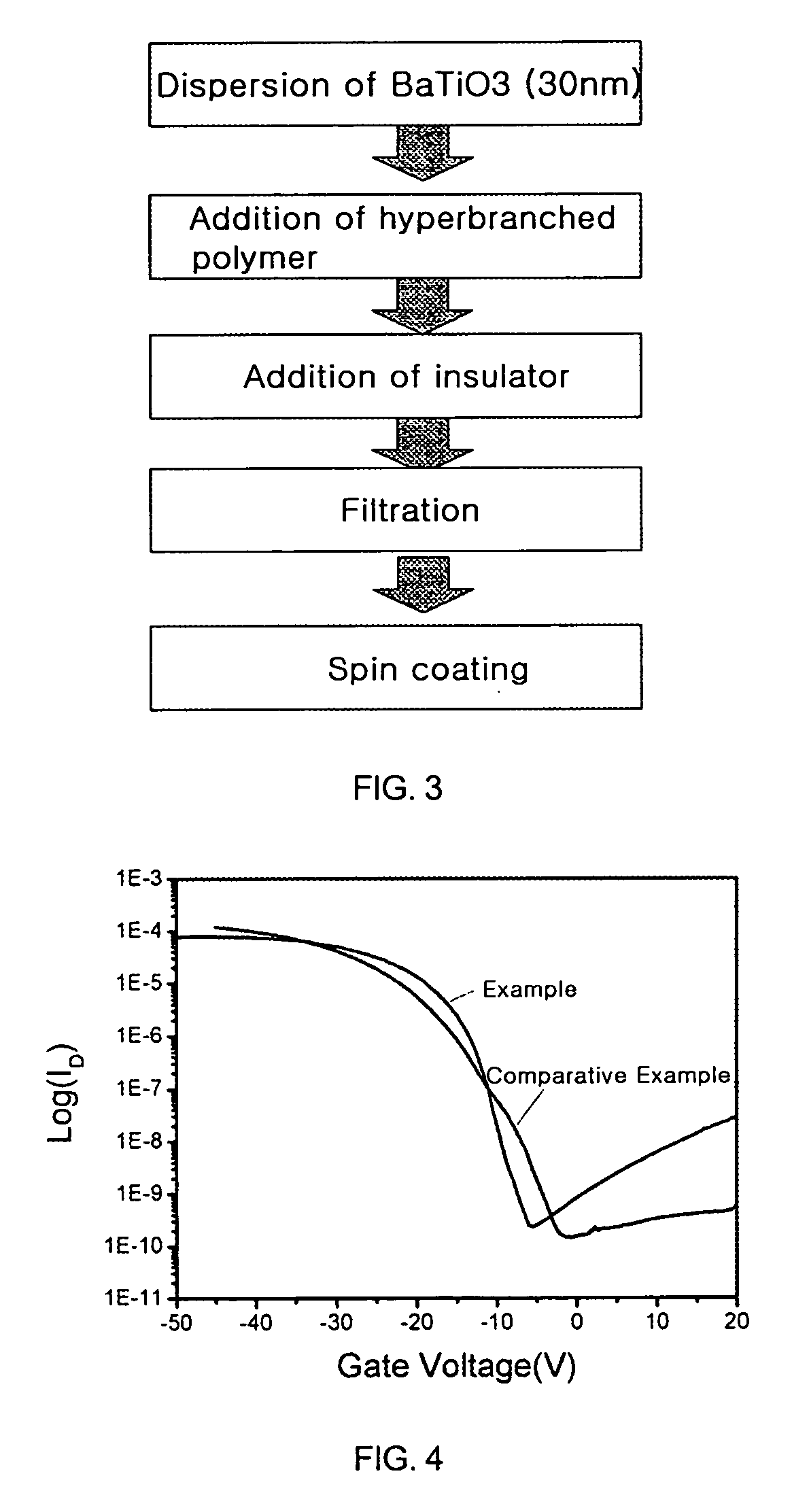
Fabrication of OTFT
[0055] First, aluminum was deposited on a clean glass substrate to a thickness of 1,000 Å by a sputtering process to form a gate electrode. Thereafter, the insulator composition prepared in Preparative Example 1 was coated on the gate electrode by a spin coating process, and was then dried at 150° C. for one hour. Pentacene was deposited on the dried structure to a thickness of 700 Å under a vacuum of 2×10⁻⁷ torr, a substrate temperature of 50° C. and a deposition rate of 0.85 Å / sec by a thermal evaporation process, and then gold (Au) was deposited thereon to a thickness of 500 Å by sputtering to fabricate a top-contact OTFT.
PUM
| Property | Measurement | Unit |
|---|---|---|
| Percent by mass | aaaaa | aaaaa |
| Size | aaaaa | aaaaa |
| Area | aaaaa | aaaaa |
Abstract
Description
Claims
Application Information
 - R&D
- Intellectual Property
- Life Sciences
- Materials
- Tech Scout
- Unparalleled Data Quality
- Higher Quality Content
- 60% Fewer Hallucinations
Browse by: Latest US Patents, China's latest patents, Technical Efficacy Thesaurus, Application Domain, Technology Topic, Popular Technical Reports.
© 2025 PatSnap. All rights reserved.Legal|Privacy policy|Modern Slavery Act Transparency Statement|Sitemap|About US| Contact US: help@patsnap.com