Materials for electronic devices

A technology of atoms and groups, applied in the direction of electric solid devices, light-emitting materials, electrical components, etc., can solve the problems of thermal stability, non-evaporation, and high technical complexity of OLED manufacturing.

Active Publication Date: 2013-06-12
MERCK PATENT GMBH
View PDF97 Cites 7 Cited by
  • Summary
  • Abstract
  • Description
  • Claims
  • Application Information

AI Technical Summary

Problems solved by technology

However, these compounds are not thermally stable and cannot be evaporated without decomposition, whi

Method used


Image

  • Materials for electronic devices
  • Materials for electronic devices
  • Materials for electronic devices

Examples


Embodiment

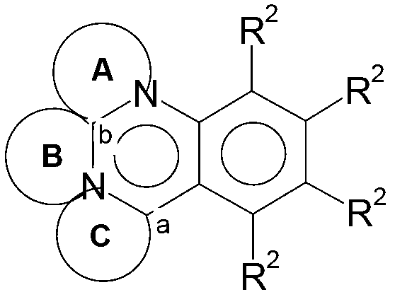
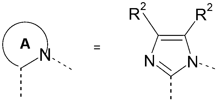
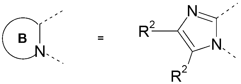
[0230] Synthesis Example 1: 4-[4-(10-Phenylanthracene-9-yl)phenyl]-6,7,11b-Triazabenzo[c]fluorene

[0231] first step:

[0232]

[0233]First, 4000 ml of water and 648.0 g (6.0 mol) of o-phenylenediamine were introduced into a 6 L four-necked flask equipped with a mechanical stirrer, internal thermometer, dropping funnel and reflux condenser. Starting from room temperature, 369 g (6.3 mol) of cyanogen chloride were added dropwise from the dropping funnel under stirring in a cooling bath (acetone / dry ice) during 15 minutes, during which time the internal temperature of the reaction mixture increased to about 65°C. The pH was then adjusted to about 9 using 550 g of 45% sodium hydroxide solution and the mixture was cooled to 15°C in a cooling bath with stirring. The solid was filtered off, rinsed with ice water, and the 2-aminobenzimidazole was dried. Yield: 750 g (94%).

[0234] Step two:

[0235]

[0236] In a 2-L four-necked flask with a protective gas inlet, reflux...


PUM


Abstract

The present invention relates to compounds according to formula (I), the use of the compounds in electronic devices, a method for production of the compounds, and electronic devices containing the compounds, preferably as electron transport materials, as hole blocking materials, as matrix materials and/or as emitter materials.

Description

technical field [0001] The present invention relates to compounds of formula (I) and to their use as functional materials in electronic devices, wherein said compounds are preferably used as electron transport materials, as hole blocking materials, as matrix materials and / or as Luminous material. Furthermore, the present invention relates to processes for the preparation of compounds of formula (I) and to electronic devices comprising said compounds of formula (I). Background technique [0002] Organic semiconducting materials, such as the compounds according to the invention, are being developed for use in many different applications in electronic devices. The structures of organic electroluminescent devices (OLEDs) in which the compounds according to the invention can be used as functional materials are described, for example, in US Pat. No. 4,539,507, US Pat. [0003] Especially considering the wide commercial use, further improvements are still needed in terms of the p...

Claims


Application Information

Patent Timeline
IPC IPC(8): C07D487/04C09K11/06H05B33/10
CPCC07D487/04Y02E10/549C09K11/06H05B33/10H10K85/6572H10K50/16H10K85/615H10K85/626
Inventor 约亨·施魏格尔海因里希·贝克尔
Owner MERCK PATENT GMBH
Why Eureka
Try Eureka