High dielectric constant grid dielectric material forming method and a semiconductor device

A technology of high dielectric constant material and gate dielectric material, applied in semiconductor devices, semiconductor/solid-state device manufacturing, electrical components, etc., to improve roughness and quality, and improve charge carrier mobility

Active Publication Date: 2009-05-06
TAIWAN SEMICON MFG CO LTD
View PDF1 Cites 5 Cited by
  • Summary
  • Abstract
  • Description
  • Claims
  • Application Information

AI Technical Summary

Problems solved by technology

[0012]The challenge here is to optimize the quality of the interfacial layer between the semiconductor wafer substrate (especially a silicon dioxide waf

Method used


Image

  • High dielectric constant grid dielectric material forming method and a semiconductor device
  • High dielectric constant grid dielectric material forming method and a semiconductor device
  • High dielectric constant grid dielectric material forming method and a semiconductor device

Examples


Embodiment Construction

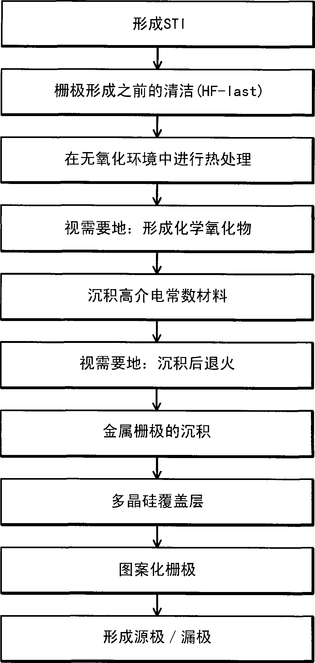
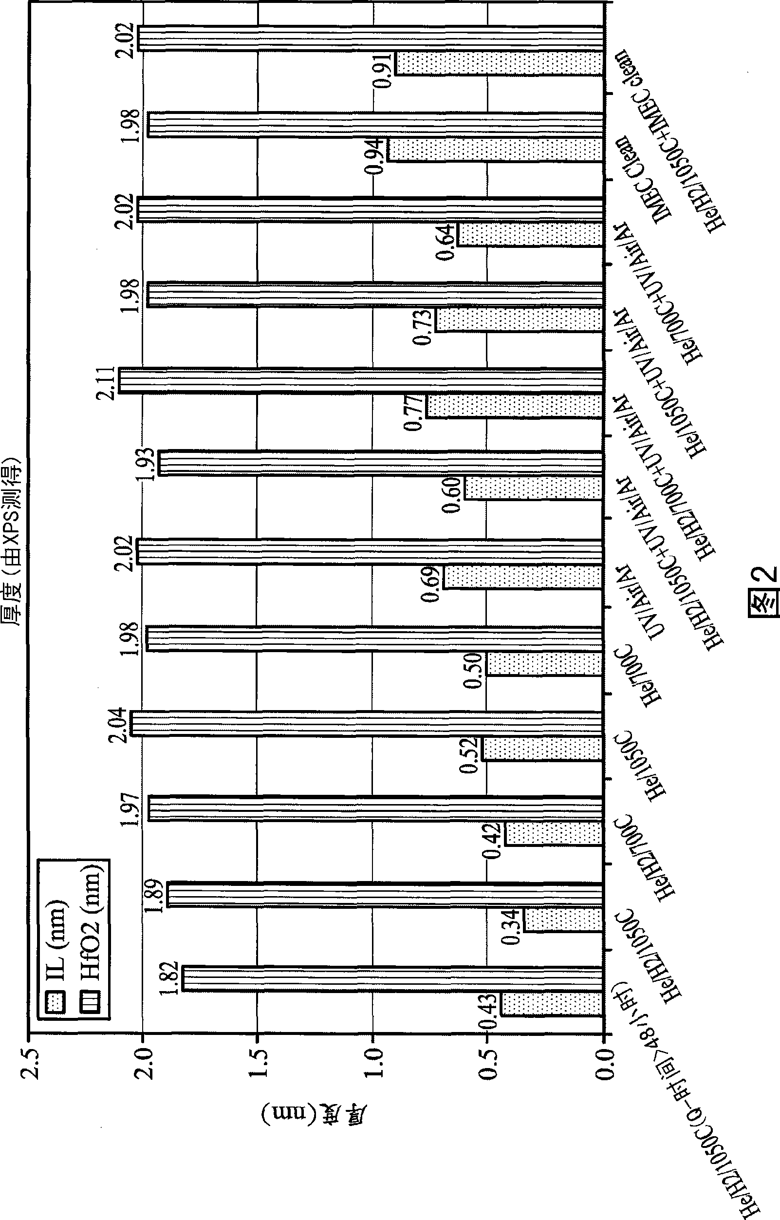
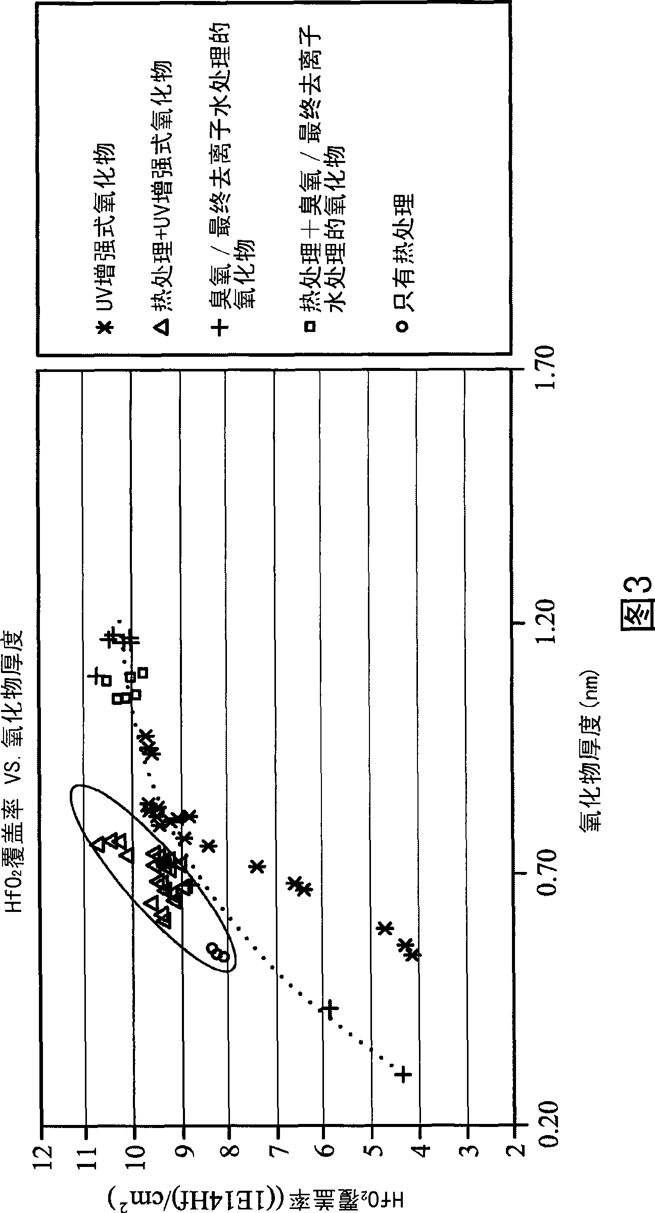
[0043] The present invention is based on the unexpected discovery that a method for carrying out the present invention comprises thermally treating in a non-oxidizing environment containing a passivating gas to form a thin interfacial layer.

[0044] The so-called "oxidative-free environment" in the present invention refers to an environment without oxygen. This environment preferably includes an inert gas environment or inert gas mixture, and optionally other additives.

[0045] In particular, the addition of hydrogen in an oxygen-free environment containing a passivation gas environment or a passivation gas mixture can increase the surface smoothness of the thin interfacial layer described above.

[0046] In the present invention, the step of heat treatment is performed after cleaning the substrate and before depositing the high dielectric constant material.

[0047] The so-called "high dielectric constant" of the present invention refers to any dielectric material, which h...


PUM

PropertyMeasurementUnit
Thicknessaaaaaaaaaa

Abstract

This invention provides a method for forming grid dielectric material with high permittivity and a semiconductor component. The method comprises following steps: providing a semiconductor substrate; cleaning the substrate; performing a thermal treatment; performing a high-k dielectric material deposition, wherein said thermal treatment step is performed in a non-oxidizing ambient, leading to the formation of a thin interfacial layer. The method of this invention can generate a uniform and thin interface layer having proper tail end so as to make it be compatible with the subsequent deposition of the high-k dielectric material deposition, and it can improve the roughness and the quality of the interface layer. At the same time, the structure of this invention can improve the electric load current carrier migration rate in the semiconductor component.

Description

technical field [0001] The present invention relates to a method for preparing an integrated circuit, and more particularly to a method for depositing a high dielectric constant material on a substrate, thereby providing an interface layer suitable for the deposition of the high dielectric constant material, and also relates to preparing a gate dielectric structure method for depositing high dielectric constant materials. Background technique [0002] There is currently a need to shrink (reduce) the size of semiconductor components to increase component density over semiconductor chips so that the semiconductor components operate faster and consume less power. [0003] Silicon dioxide is most commonly used as the gate dielectric material for semiconductor components. However, when silicon dioxide is used as a gate dielectric material, as the silicon dioxide thickness decreases, there is an accompanying severe restriction on the oxidation process. When using these dielectri...

Claims


Application Information

Patent Timeline
IPC IPC(8): H01L21/28H01L21/31H01L29/51H01L29/78
CPCH01L21/31645H01L21/28211H01L21/3141H01L21/31654H01L29/513H01L21/28167H01L21/28194H01L21/02057H01L29/517H01L21/02178H01L21/02266H01L21/0228H01L21/02192H01L21/02197H01L21/02156H01L21/02269H01L21/02189H01L21/02186H01L21/02181H01L21/02255H01L21/02236H01L21/02238H01L21/02148H01L21/0206H01L29/42364
Inventor 欧阳晖尚·路克·艾佛拉特萝拉·宁斯莉塔·沃斯
Owner TAIWAN SEMICON MFG CO LTD
Why Eureka
Try Eureka