Perovskite-based X-ray detector with p-i-n structure and preparation method thereof
A p-i-n, photodetector technology, applied in semiconductor/solid-state device manufacturing, photovoltaic power generation, electric solid-state devices, etc., can solve problems such as high dark current, achieve high charge carrier mobility, optimize energy level matching relationship, The effect of high X-ray absorption efficiency
- Summary
- Abstract
- Description
- Claims
- Application Information
AI Technical Summary
Problems solved by technology
Method used
Image

Examples
preparation example Construction
[0070] The second aspect of the embodiment of the present application provides a method for preparing a p-i-n structure perovskite-based X-ray detector, including the following steps:
[0071] S10. Obtain a conductive substrate, and prepare a first semiconductor layer on the conductive substrate;
[0072] S20. preparing a perovskite active layer on the surface of the first semiconductor layer away from the conductive substrate;
[0073] S30. Prepare a second semiconductor layer on the surface of the perovskite active layer away from the first semiconductor layer;
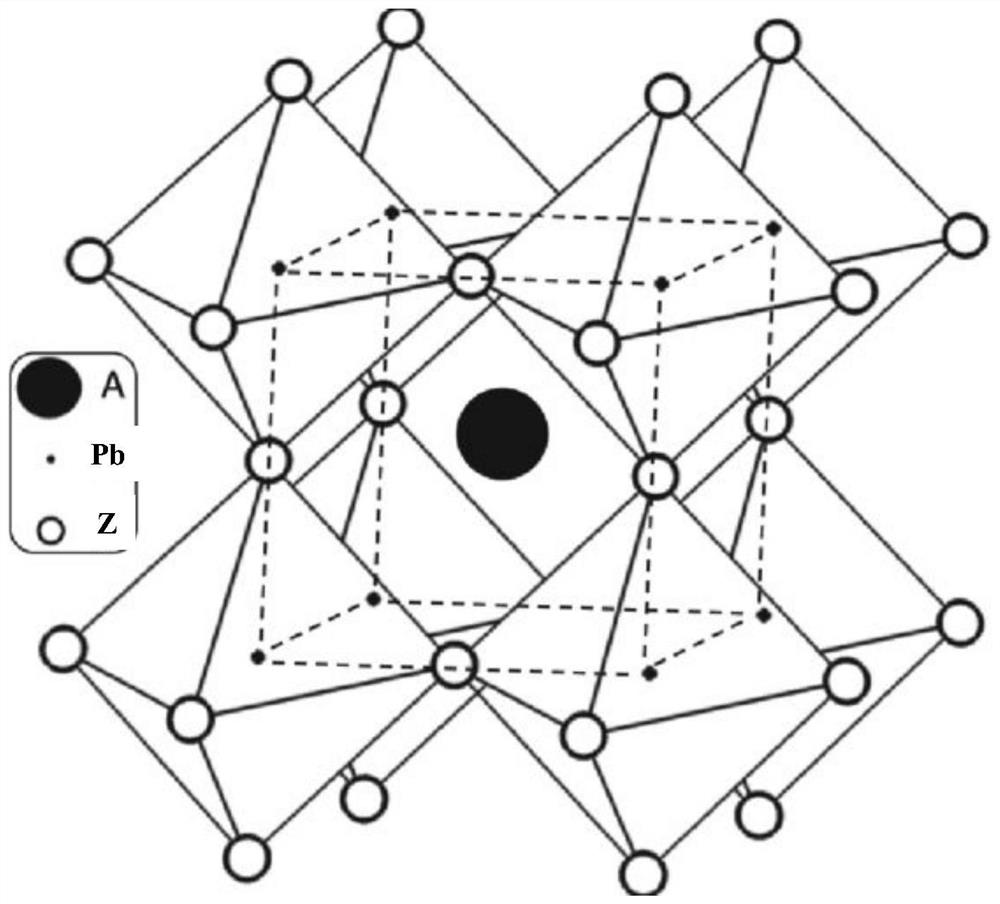
[0074] S40. Prepare a back electrode on the surface of the second semiconductor layer away from the perovskite active layer to obtain a p-i-n structure perovskite-based X-ray detector; wherein, the first semiconductor layer and the second semiconductor layer respectively contain p-type functional materials or n Type functional materials; the perovskite active layer contains a chemical formula of APbZ 3 A halide pe...
Embodiment 1
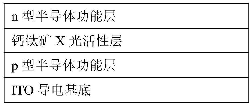
[0100] A p-i-n structure perovskite-based X-ray detector, the structure is as attached figure 2 Shown, its preparation comprises steps:
[0101] 1. Ni(NO 3 ) 2 ·6H 2 O (0.5mol) was dissolved in 100mL deionized water, by using NaOH solution (10molL -1 ) to adjust the pH of the solution system to 10 to obtain a colloidal precipitate; then, after washing twice with water, dry at 80° C. for 6 hours to obtain a green powder; and then calcinate at 270° C. for 2 hours to obtain a dark black nickel oxide nanocrystalline powder. Using water as a dispersant, configuring nickel oxide into a slurry with a mass fraction of 70% to obtain a nickel oxide slurry;
[0102] 2. On the conductive substrate of indium tin oxide ITO transparent glass, scrape-coat nickel oxide slurry, that is, the slurry of the p-type functional layer. The scraping speed is 10mm / s, and the height of the scraper is 30μm. The amount of scraping on the surface of the substrate is 100 μL / (1 inch×3 inch); then dry at...
Embodiment 2
[0107] A p-i-n structure perovskite-based X-ray detector, the difference between it and embodiment 1 is that the perovskite material used in step 3 is CH 2 (NH 3 ) 2 PB 3 .
PUM
| Property | Measurement | Unit |
|---|---|---|
| Thickness | aaaaa | aaaaa |
| Thickness | aaaaa | aaaaa |
| Thickness | aaaaa | aaaaa |
Abstract
Description
Claims
Application Information
 - R&D
- Intellectual Property
- Life Sciences
- Materials
- Tech Scout
- Unparalleled Data Quality
- Higher Quality Content
- 60% Fewer Hallucinations
Browse by: Latest US Patents, China's latest patents, Technical Efficacy Thesaurus, Application Domain, Technology Topic, Popular Technical Reports.
© 2025 PatSnap. All rights reserved.Legal|Privacy policy|Modern Slavery Act Transparency Statement|Sitemap|About US| Contact US: help@patsnap.com