Check patentability & draft patents in minutes with Patsnap Eureka AI!

Semiconductor device and method of manufacturing the same

Active Publication Date: 2014-01-02
SK HYNIX INC +1
View PDF1 Cites 21 Cited by
  • Summary
  • Abstract
  • Description
  • Claims
  • Application Information

AI Technical Summary

Benefits of technology

The present invention provides a method of manufacturing a semiconductor device using two different gate metals to prevent failure in metal etching. The semiconductor device is formed with a dual-work function gate, which has work functions of an NMOS and a PMOS, through adjustment of the N, Al and Ti contents within a TiN electrode. This allows for realization of a high performance CMOS device. The method of manufacturing the semiconductor device includes the formation of a Ti-rich TiN layer for an nMOSFET and an N-rich TiN layer for a pMOSFET through adjustment of the N and Ti contents in the TiN electrode, which prevents etching failure of metal electrodes in formation of a CMOS device. The method also includes the formation of an electrode having two metal work functions for a CMOSFET using a single material, that is, TiN or TiAlN, which prevents etching failure of metal electrodes and achieves equivalent oxide thickness (EOT) scaling and greater shift of the flat band voltage (VFB) than an existing CMOS process using Al2O3 capping.

Problems solved by technology

However, reduction in design rule of semiconductor devices results in increase in gate leakage current, causing a limit of the silicon oxide layer.
To obtain symmetrical and low threshold voltages in formation of a complementary metal-oxide semiconductor (CMOS), a technology using two metals having ideal work functions of an NMOS and a PMOS is suggested, but has a problem of causing etching failure of a metal electrode.
In particular, metals such as Ru, Mo, Pt, and the like, which can be used for an electrode of a PMOS and have high work functions, are not suited to a gate first process due to etching difficulty and low thermal stability.
However, it has been reported that TiN has an insufficient work function to be used for nMOSFETs and pMOSFETs.

Method used


Image

  • Semiconductor device and method of manufacturing the same
  • Semiconductor device and method of manufacturing the same
  • Semiconductor device and method of manufacturing the same

Examples


first embodiment

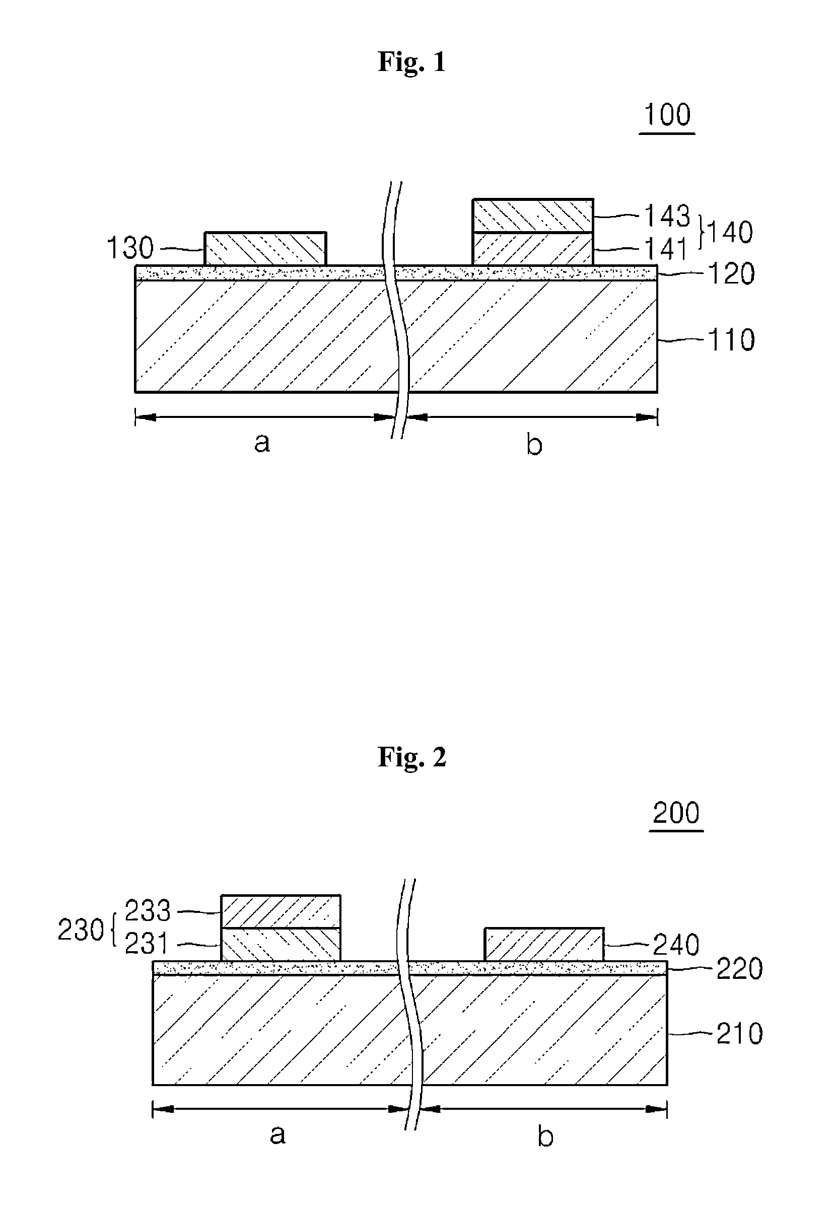
[0033]FIG. 1 is a sectional view of a semiconductor device in accordance with the present invention.

[0034]Referring to FIG. 1, a semiconductor device 100 includes a substrate 110, a gate insulation layer 120, a first metal gate electrode 130, and a second metal gate electrode 140.

[0035]The substrate 110 is defined by a first region (a) and a second region (b). The first region (a) refers to an n-channel metal oxide semiconductor (NMOS) region and the second region (b) refers to a p-channel metal oxide semiconductor (PMOS) region. The first region (a) and the second region (b) are isolated from each other by a field oxide layer (not shown) or a shallow trench isolation layer (STI, not shown).

[0036]The substrate 110 may be a typical semiconductor substrate. By way of example, the substrate 110 may be a p-type substrate doped with a low density of p-type impurities or an n-type substrate doped with a low density of n-type impurities. Alternatively, the substrate 110 may be a bulk Si su...

second embodiment

[0049]FIG. 2 is a sectional view of a semiconductor device in accordance with the present invention.

[0050]Referring to FIG. 2, a semiconductor device 200 includes a substrate 210, a gate insulation layer 220, a first metal gate electrode 230, and a second metal gate electrode 240.

[0051]Here, each of the first and the second metal gate electrodes 230, 240 are formed of TiN material but may have different compositions. Here, the first metal gate electrode 230 has a stack structure of a Ti-rich TiN layer 231 and an N-rich TiN layer 233. The first metal gate electrode 230 is formed of a Ti-rich TiN layer, which has a higher Ti content than that the second metal gate electrode 240. On the other hand, the second metal gate electrode 240 has a lower thickness than the first metal gate electrode 230 and is formed of a single N-rich TiN layer.

[0052]In the first and second metal gate electrodes 230, 240, the work functions of the TiN electrodes are adjusted according to the N and Ti contents,...

third embodiment

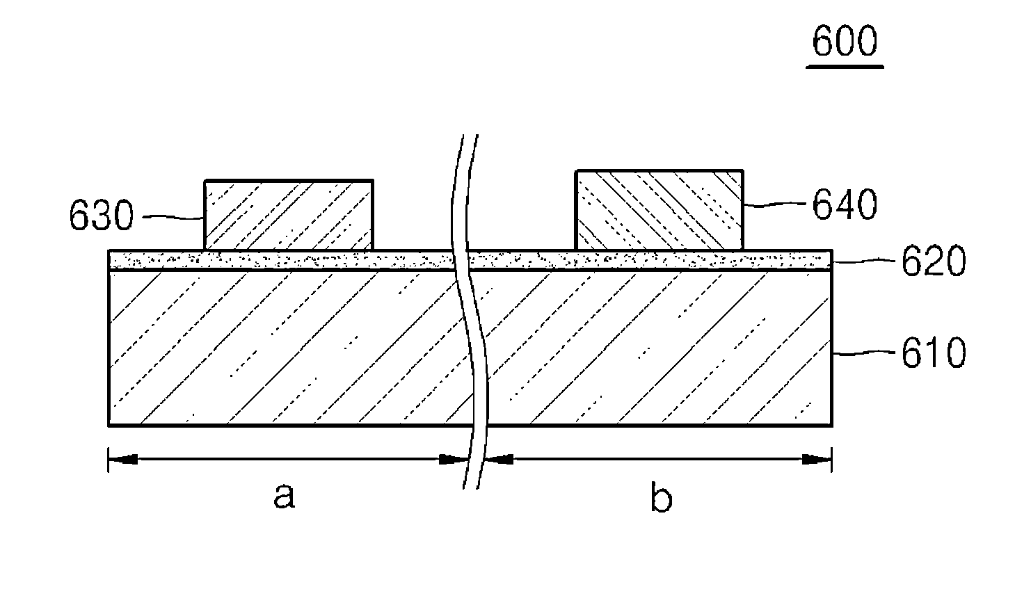
[0066]FIG. 6 is a sectional view of a semiconductor device in accordance with the present invention.

[0067]Referring to FIG. 6, a semiconductor device 600 includes a substrate 610, a gate insulation layer 620, a first metal gate electrode 630, and a second metal gate electrode 640.

[0068]In this embodiment, the first metal gate electrode 630 is formed on the gate insulation layer 620 of the first region (a) corresponding to an NMOS region, and the second metal gate electrode 640 is formed on the gate insulation layer 620 of a second region (b) corresponding to a PMOS region and has a higher thickness than the first metal gate electrode 630.

[0069]The first and the second metal gate electrodes 630, 640 according to the third embodiment may be formed of single layers of titanium aluminum nitride (TiAlN) material, but with different compositions.

[0070]Here, the first metal gate electrode 630 is formed of an Al / Ti-rich TiAlN layer, the Al and Ti contents of which are higher than those of t...


PUM


Abstract

The present disclosure relates to a semiconductor device and a method of manufacturing the same. The semiconductor device may include a first metal gate electrode provided in a NMOS region of a substrate; and a second metal gate electrode provided in a PMOS region of the substrate, wherein the first and second metal gate electrodes may be formed of TiN material or TiAlN material. Here, the first metal gate electrode may have a higher titanium (Ti) content than the second metal gate electrode, and the second metal gate electrode may have a higher nitrogen (N) content than the first metal gate electrode.

Description

CROSS-REFERENCE TO RELATED APPLICATION[0001]This application claims the benefit under 35 U.S.C. §119 of Korean Patent Application No. 10-2012-0070913, filed on Jun. 29, 2012 in the Korean Intellectual Property Office, the entirety of which is incorporated herein by reference.BACKGROUND[0002]1. Technical Field[0003]The present invention relates to semiconductor devices, and more particularly, to a semiconductor device of a CMOS structure, which includes a dual-work function metal gate having work functions adjusted by controlling a composition of components such as nitrogen (N), aluminum (Al), and titanium (Ti) within a TiN electrode, and a method of manufacturing the same.[0004]2. Description of the Related Art[0005]In a semiconductor device, a silicon oxide layer (SiO2) is generally used as a gate dielectric layer of memories and logics. However, reduction in design rule of semiconductor devices results in increase in gate leakage current, causing a limit of the silicon oxide layer...

Claims


Application Information

Patent Timeline
IPC IPC(8): H01L27/092H01L21/8238
CPCH01L27/092H01L21/823828H01L21/823842H01L21/28008H01L21/8238H01L27/0922H01L29/4966
Inventor CHOI, CHANG-HWAN
Owner SK HYNIX INC
Features
  • R&D
  • Intellectual Property
  • Life Sciences
  • Materials
  • Tech Scout
  • Unparalleled Data Quality
  • Higher Quality Content
  • 60% Fewer Hallucinations
Learn More