Light emitting device

a technology of light-emitting devices and semiconductors, which is applied in the direction of semiconductor devices, electrical equipment, basic electric elements, etc., can solve the problems of affecting the soldering strength of the device, the risk of cracking or chipping of the substrate, etc., and achieve the effect of good soldering strength

Active Publication Date: 2015-11-26
NICHIA CORP
View PDF1 Cites 20 Cited by
  • Summary
  • Abstract
  • Description
  • Claims
  • Application Information

AI Technical Summary

Benefits of technology

[0007]An object of the present disclosure is to provide a light emitting device with which good soldering strength can be obtained while maintaining the mechanical strength of even a thin base body.

Problems solved by technology

With this LED module, however, the solder fillet on the edges of the substrate caused the ends of the substrate to be thin, so there was a risk of cracking or chipping of the substrate.
This problem was particularly pronounced when the LED module was flatter (thinner).

Method used


Image

  • Light emitting device
  • Light emitting device
  • Light emitting device

Examples


embodiment 1

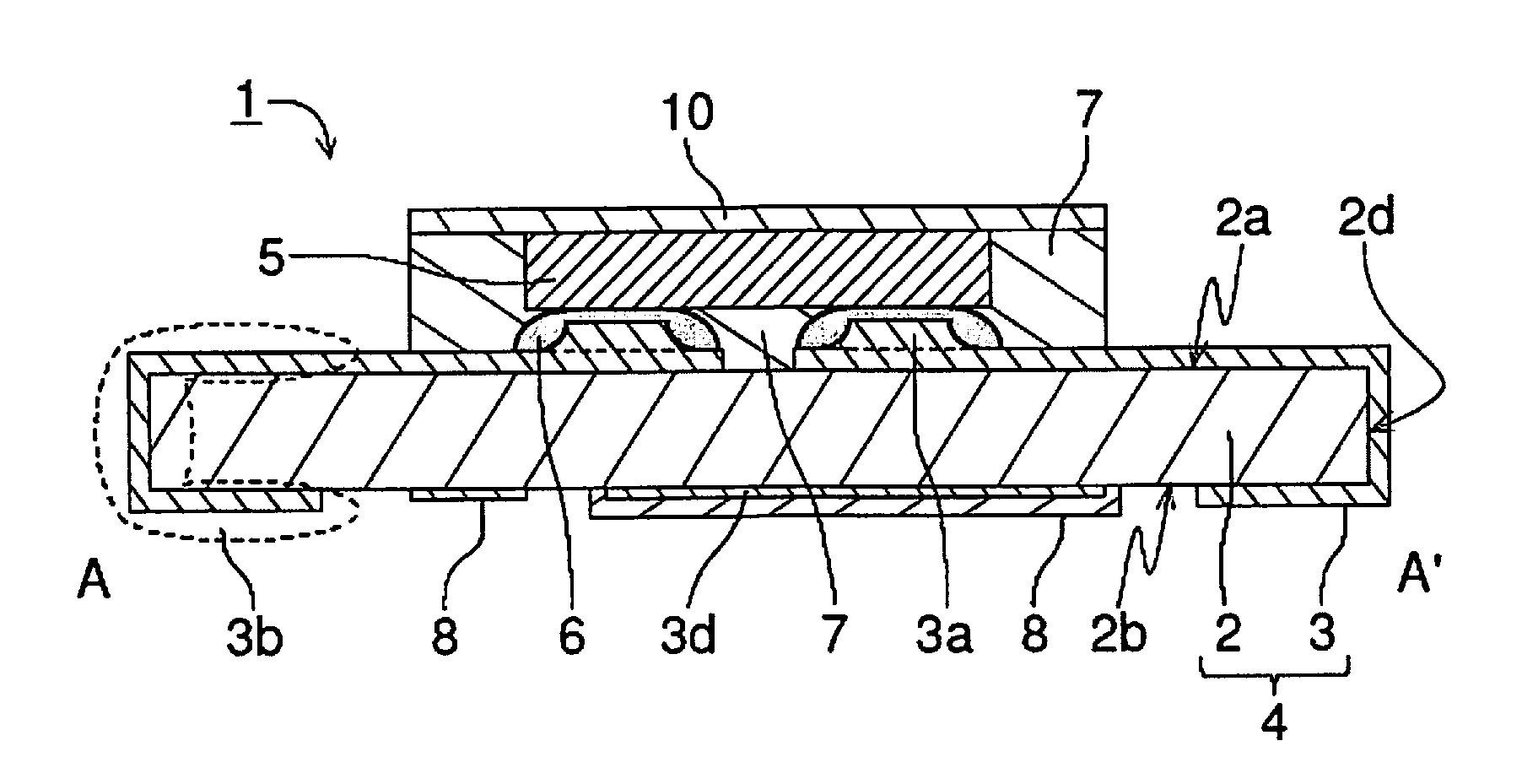
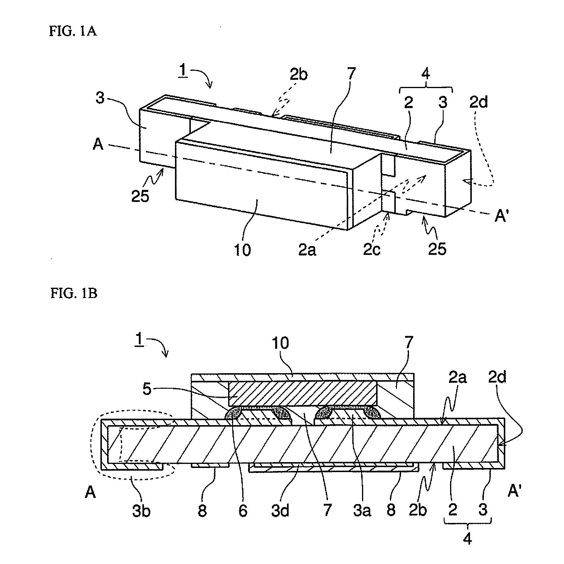
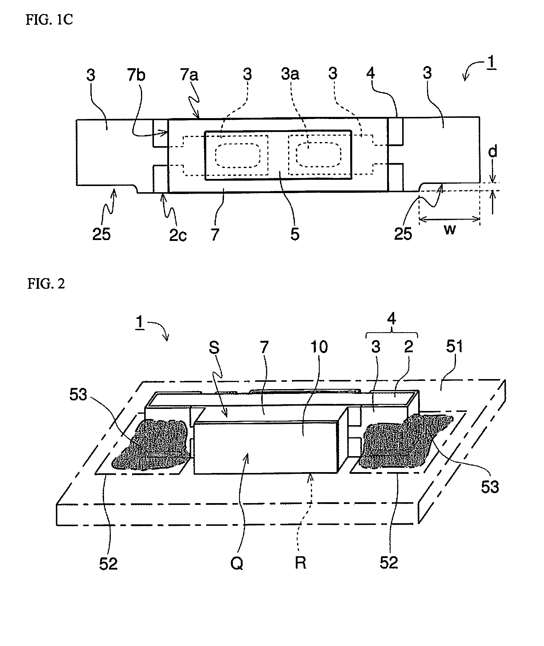
[0137]As shown in FIGS. 1A to 1C, the light emitting device 1 in this embodiment is constituted by the base body 4, the light emitting element 5, and the sealing member 7. The base body 4 has the base material 2 and the connection terminals 3. The base material 2 includes a first main face 2a having a lengthwise direction and a short-side direction that is perpendicular to said lengthwise direction, a second main face 2b on the opposite side from the first main face 2a, and first end face 2c that extends in the lengthwise direction, and a second end face 2d that extends in the short-side direction. The connection terminals 3 consist of at least a positive and negative pair, and are provided on the first main face 2a of the base material. The connection terminals 3 are formed by laminating Cu / Ni / Au (total thickness: 20 μm, linear expansion coefficient: about 20 ppm / ° C.) from the base material 2 side, and are formed on a surface of the base material 2, i.e. an upper surface as a firs...

embodiment 2

[0164]As shown in FIGS. 4A to 4C, the light emitting device 21 in this embodiment is constituted by a base body 24 having connection terminals 23, a plurality of light emitting elements 5, and a sealing member 27. The connection terminals 23 are disposed extending to the top face, the end faces, and the bottom face on both sides in the lengthwise direction of a base material 22. On the top face of the base material 22 is further disposed a terminal 29 that allows the light emitting elements 5 to be connected serially, for example. On one face of the base body 24, the connection terminals 23 and the terminal 29 each have a protrusion pattern 23a serving as an element connection section, and on these protrusion patterns 23a, the light emitting elements 5 are flip-chip mounted with a fusible joining member 6.

[0165]The light emitting elements 5 are disposed so that they are arranged in a single line, but they need not be in a single line, and may instead be disposed in columns and rows....


PUM


Abstract

A light emitting device including; a base body having a base material that includes a first main face that has a lengthwise direction and a short-side direction that is perpendicular to the lengthwise direction, a second main face on the opposite side from the first main face, a first end face that extends in the lengthwise direction, and a second end face that extends in the short-side direction, and connection terminals that are provided on the first main face of the base material; and a light emitting element that is installed on the first main face and is connected to the connection terminals, the first end face of the base material has a recess that is contiguous with the first main face and the second end face and/or is contiguous with the second main face and the second end face, a length of the recess in a lengthwise direction is greater than a depth in a short-side direction, and the connection terminals are provided extending over the recess.

Description

CROSS-REFERENCE TO RELATED APPLICATIONS[0001]This application claims priority to Japanese Patent Application No. 2014-105131 filed on May 21, 2014. The entire disclosure of Japanese Patent Application No. 2014-105131 is hereby incorporated herein by reference.BACKGROUND[0002]1. Field of the Invention[0003]The present disclosure relates to a light emitting device.[0004]2. Description of Related Art[0005]An LED module has been proposed in the past in which a solder fillet in the shape of a hollow quarter-cylinder was provided to the edge of a substrate on the top face of which was disposed a light emitting diode (LED) chip (see. JP 2012-504318 A, for example).[0006]With this LED module, however, the solder fillet on the edges of the substrate caused the ends of the substrate to be thin, so there was a risk of cracking or chipping of the substrate. This problem was particularly pronounced when the LED module was flatter (thinner).SUMMARY[0007]An object of the present disclosure is to p...

Claims


Application Information

Patent Timeline
Patent Type & Authority Applications(United States)
IPC IPC(8): H01L33/62H01L33/48
CPCH01L33/486H01L33/62H01L24/97H01L33/642H01L2224/16225
Inventor TAMAKI, HIROTONAKABAYASHI, TAKUYA
Owner NICHIA CORP
Why Eureka
Try Eureka