Electronic component and manufacturing method of electronic component

a manufacturing method and electronic component technology, applied in semiconductor/solid-state device testing/measurement, semiconductor/solid-state device details, instruments, etc., can solve the problem of insufficient strength in soldering joints, inability to make external electrodes on side surfaces before cutting process, and difficulty in precisely forming the shape, dimensions and position of each external electrode.

Active Publication Date: 2010-06-24
TDK CORPARATION
View PDF18 Cites 129 Cited by
  • Summary
  • Abstract
  • Description
  • Claims
  • Application Information

AI Technical Summary

Benefits of technology

[0011]It is therefore an object of the present invention to provide an electronic component having external electrodes with a large electrode area so that enough soldering strength is available when mounting the electronic component, and to provide a manufacturing method of the electronic component.

Problems solved by technology

However, because no side surface of the chip will expose before cutting the substrate into the individual chips, it is impossible to make the external electrodes on the side surfaces before the cutting process.
If no external electrode is formed on the side surfaces, an area of the electrodes becomes extremely small and thus enough strength cannot be ensured in soldering joint.
Since it is necessary to form the external electrode pattern after having separated into individual chips, according to the conventional art, it is very difficult to precisely form the shape, dimensions and position of each external electrode.
In addition, according to the conventional art, because a plurality of fabrication processes such as a process for fabricating elements on a substrate and a process performed after the separation of the substrate into individual chips are necessary, the manufacturing cost will be extremely increased.

Method used


Image

  • Electronic component and manufacturing method of electronic component
  • Electronic component and manufacturing method of electronic component
  • Electronic component and manufacturing method of electronic component

Examples


Embodiment Construction

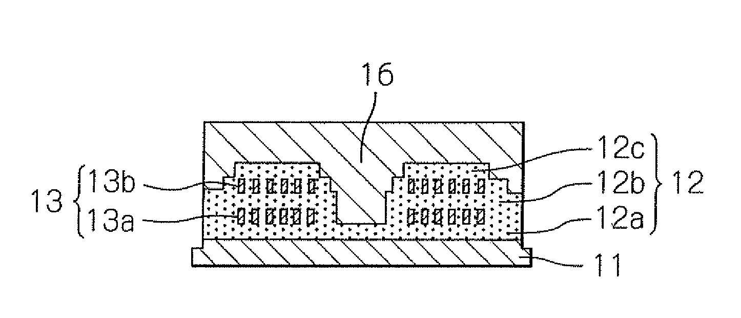
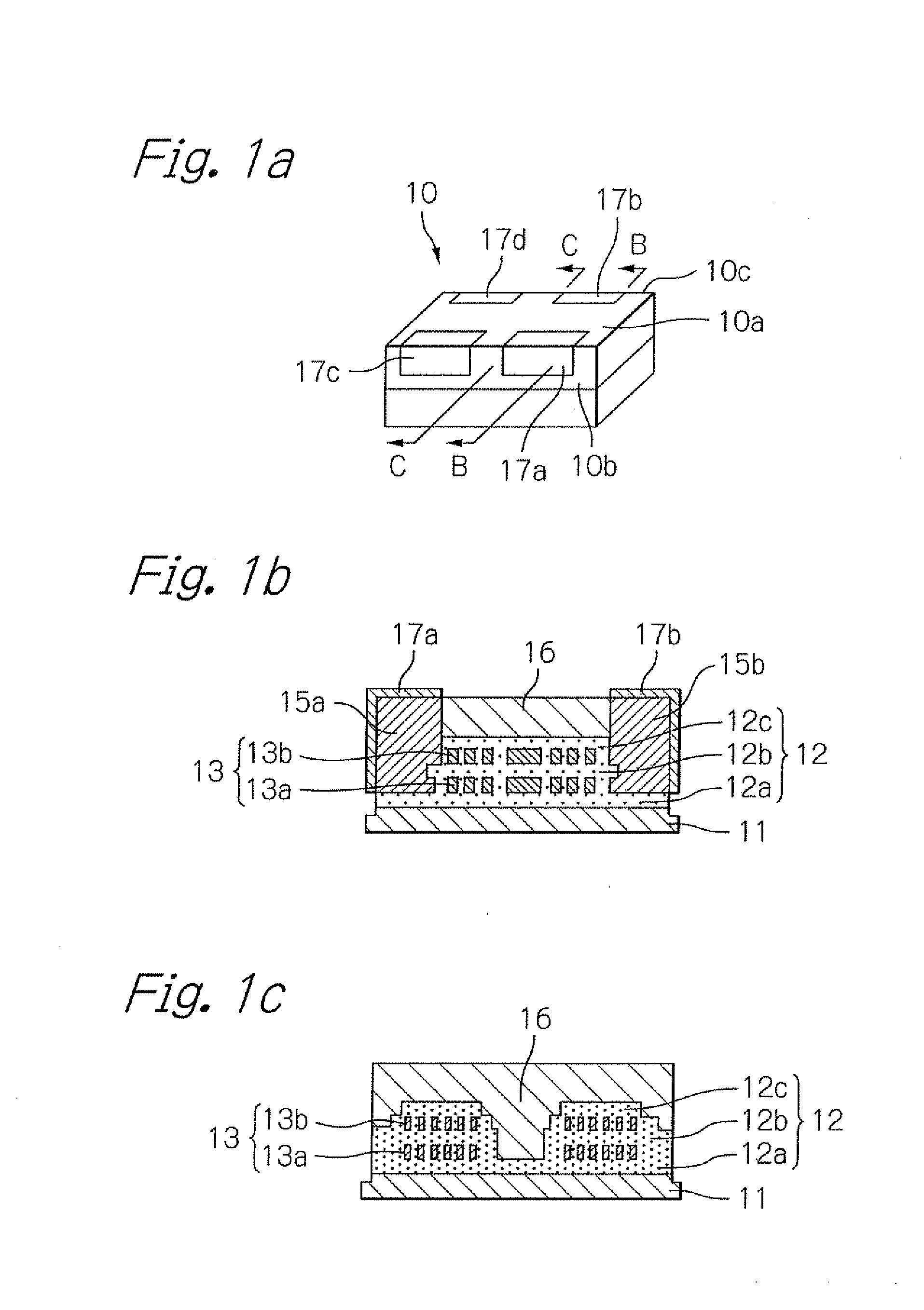
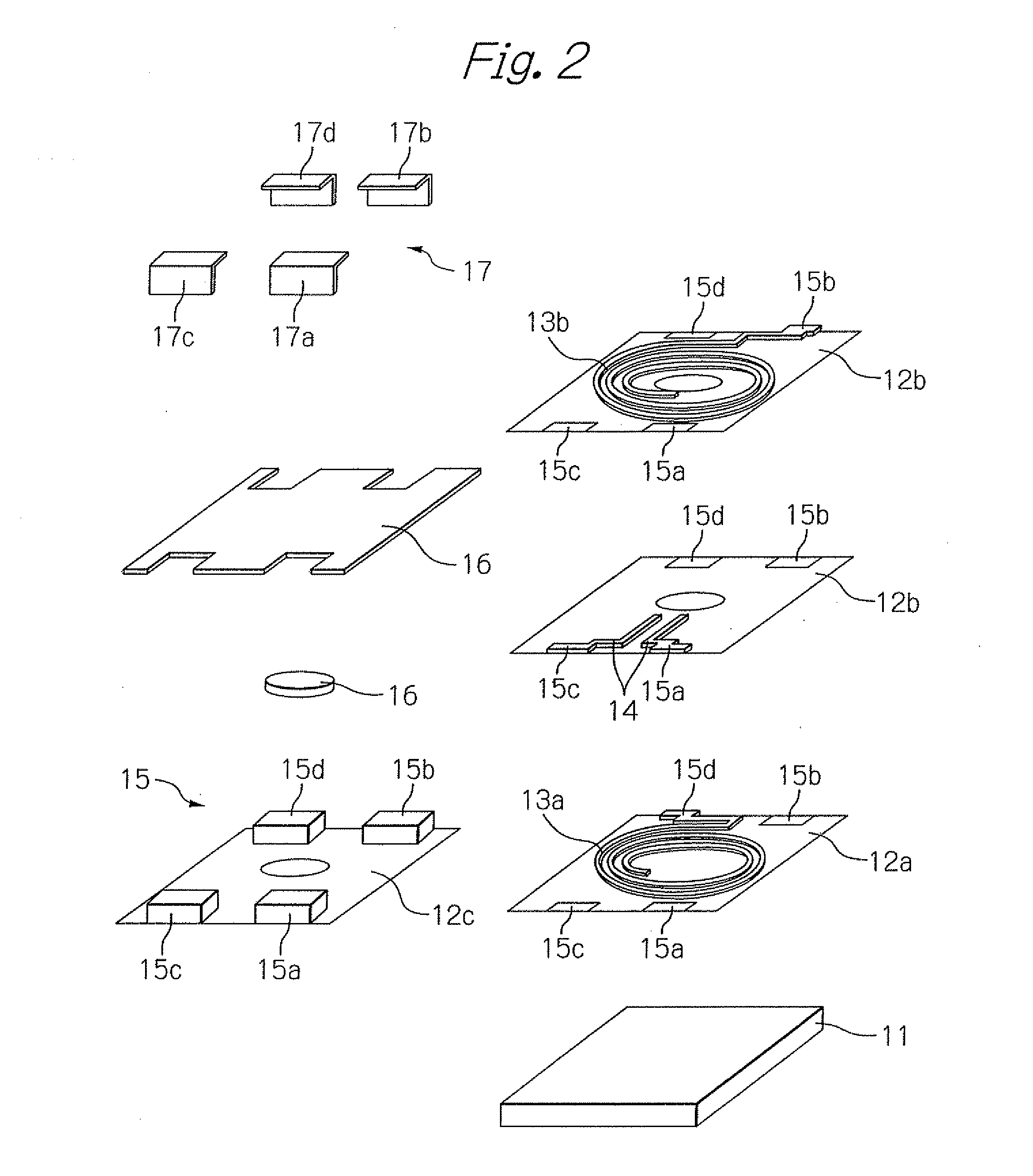
[0048]FIGS. 1a, 1b and 1c schematically illustrate configuration of a common mode choke coil as an embodiment of an electronic component according to the present invention, and FIG. 2 illustrates an exploded configuration of the common mode choke coil of this embodiment. FIG. 1a shows an external perspective view, FIG. 1b shows a B-B line section and FIG. 1c shows a C-C line section. It should be noted that the B-B line section of FIG. 1b corresponds to a section where external electrodes are existed and that the C-C line section of FIG. 1c corresponds to a section where no external electrode is existed.

[0049]In these figures, reference numeral 10 denotes a common mode choke coil, 11 denotes a ferrite substrate, 12 denotes an insulation layer laminated on the ferrite substrate 11 and configured by a first insulation film 12a, a second insulation film 12b and a third insulation film 12c, 13 denotes a coil conductor layer surrounded by the insulation layer 12 and configured by a first...


PUM

PropertyMeasurementUnit
heightaaaaaaaaaa
heightaaaaaaaaaa
thicknessaaaaaaaaaa

Abstract

A manufacturing method of electronic components includes forming a first insulation layer on a substrate, forming a plurality of passive elements on the first insulation layer, forming a second insulation layer on the passive elements, forming a plurality of conductor layers electrically connected to the respective passive elements, on the outer side of the second insulation layer to be exposed to an upper surface of each electronic component, and forming grooves between the electronic components including the respective passive elements to expose side surfaces of each electronic component and parts of the conductor layers from the side surfaces of each electronic component. The manufacturing method further including plating a plurality of external electrodes on the respective conductor layers exposed to the upper surface and the side surfaces of each electronic component, and cutting the substrate to completely separate into individual electronic components.

Description

PRIORITY CLAIM[0001]This application claims priority from Japanese patent applications No. 2008-325389 filed on Dec. 22, 2008 and No. 2009-199260 filed on Aug. 31, 2009, which are incorporated herein by reference.BACKGROUND OF THE INVENTION[0002]1. Field of the Invention[0003]The present invention relates to a surface-mounted type electronic component for surface-mounting on a printed circuit board or on a hybrid integrated circuit (HIC), which are used for an electronic equipment, and a manufacturing method of the electronic component.[0004]2. Description of the Related Art[0005]There are various passive components such as coil components configuring inductor elements or common mode choke coils or capacitor components, used as electronic components surface-mounted on electronic equipments such as computers or mobile telephones.[0006]As for the coil component for example, known are a line-wound type coil component with a ferrite core and a copper wire wound around the ferrite core, ...

Claims


Application Information

Patent Timeline
Patent Type & Authority Applications(United States)
IPC IPC(8): H05K7/02H05K3/30
CPCH01F27/027H01F27/292Y10T29/4913H01G4/224H01G4/33H01F41/046
Inventor YOSHIDA, MAKOTOKAMIYAMA, HIROSHINISHIKAWA, TOMONAGA
Owner TDK CORPARATION
Why Eureka
Try Eureka