
3-D Displaying Panel Having Depth-Of-Field Effect And Displaying Method Thereof

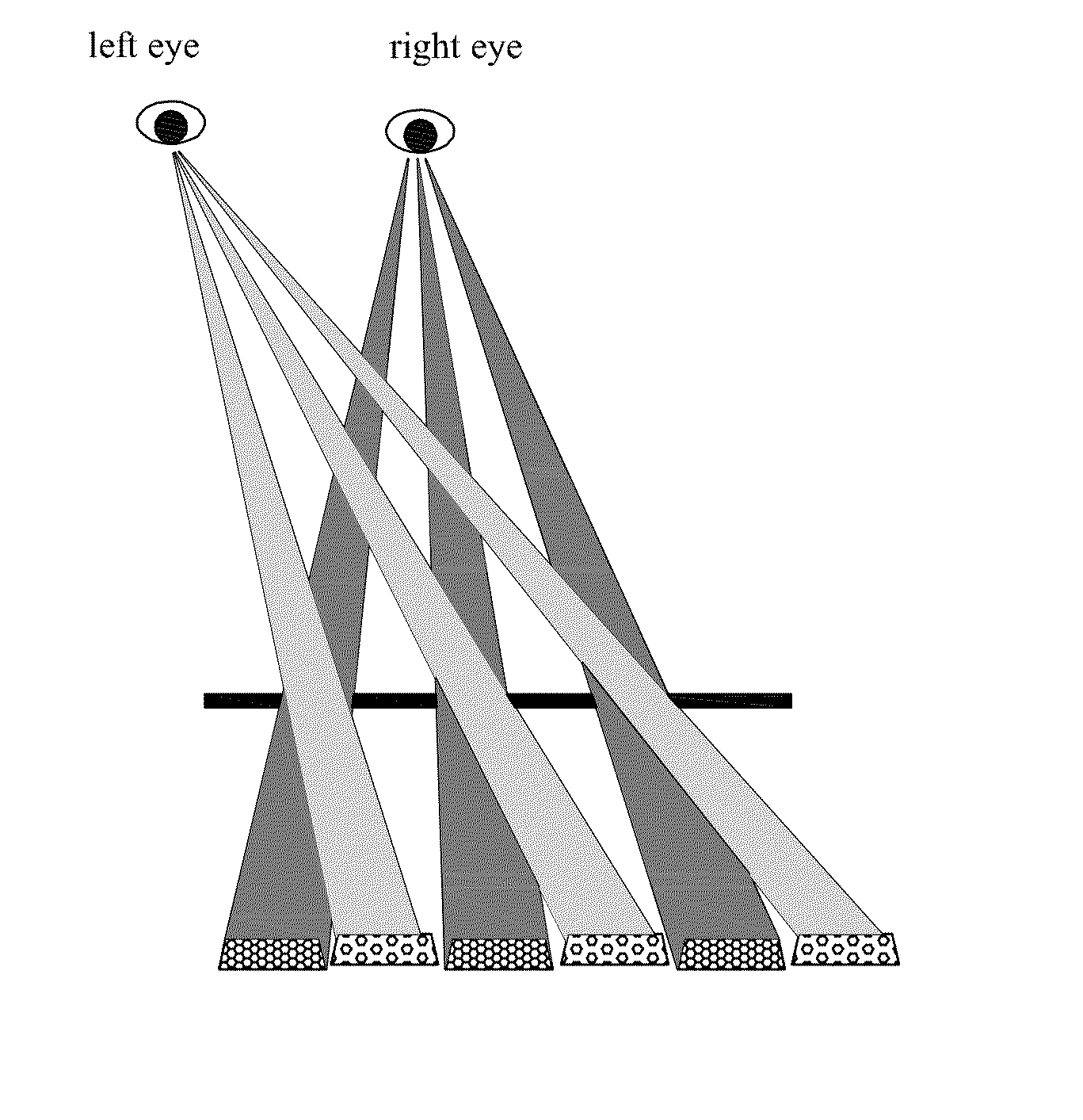
Inactive Publication Date: 2015-12-03
TCL CHINA STAR OPTOELECTRONICS TECH CO LTD
View PDF2 Cites 2 Cited by
  • Summary
  • Abstract
  • Description
  • Claims
  • Application Information

AI Technical Summary

Benefits of technology

The present invention provides a 3-D display panel with depth-of-field effect that solves the technical problem of thin-film-transistor liquid crystal display devices. The panel is cost-effective, has high brightness, quick responding time, and high contrast. It also has a larger view angle and 3-D depth-of-field effect, presenting a 3-D effect closer to our naked eye. The invention also includes a 3-D display panel and a displaying method that realizes the 3-D display by respectively displaying a near view and a father view through first and second organic light emitting layers. The invention provides a solution to the technical problem of thin-film-transistor liquid crystal display devices being limited to only 2-D display.

Problems solved by technology

This technology is relatively low cost, but the low screen brightness.
The cost is comparable low, while the brightness of the screen is also compromised.
This 3D display technology shows better results, the brightness is not affected, but its manufacturing process is not compatible to the manufacturing technology of LCD, the need to invest in new equipment and production lines.

Method used


Image

  • 3-D Displaying Panel Having Depth-Of-Field Effect And Displaying Method Thereof
  • 3-D Displaying Panel Having Depth-Of-Field Effect And Displaying Method Thereof
  • 3-D Displaying Panel Having Depth-Of-Field Effect And Displaying Method Thereof

Examples


Embodiment Construction

[0037]In order to further elaborate the manner and the results achieved by the present invention, detailed description of preferred embodiments will be given along with the accompanied drawings.

[0038]Referring to FIGS. 4 and 5, the present invention provides a 3-D display panel having depth-of-field effect, and which includes a substrate 12 and thin-film-transistor array 14 formed on the substrate 12, a first organic light emitting layer 16 formed onto the thin-film-transistor array 14, an insulative layer 17 disposed onto the thin-film-transistor array 14 and the first organic light-emitting layer 16, and a second organic light-emitting layer 18 formed onto the insulative layer 17, an cathode layer 19 disposed onto the insulative layer 17 and the second light-emitting layer 18, wherein the first light-emitting layer 16 and the second light-emitting layer 18 are offset from each other, and wherein the first organic light-emitting layer 16 displays a screen of near view, and the seco...


PUM


Abstract

The present invention provides a 3-D display panel having depth-of-field effect, and which includes a substrate (12) and thin-film-transistor array (14) formed on the substrate (12), a first organic light emitting layer (16) formed onto the thin-film-transistor array (14), an insulative layer (17) disposed onto the thin-film-transistor array (14) and the first organic light-emitting layer (16), and a second organic light-emitting layer (18) formed onto the insulative layer (17), an cathode layer (19) disposed onto the insulative layer (17) and the second light-emitting layer (18), wherein the first light-emitting layer (16) and the second light-emitting layer (18) are offset from each other, and wherein the first organic light-emitting layer (16) displays a screen of near view, and the second organic light-emitting layer (18) displays a screen of father view such that the near view and the father view are separately to display the 3-D effects.

Description

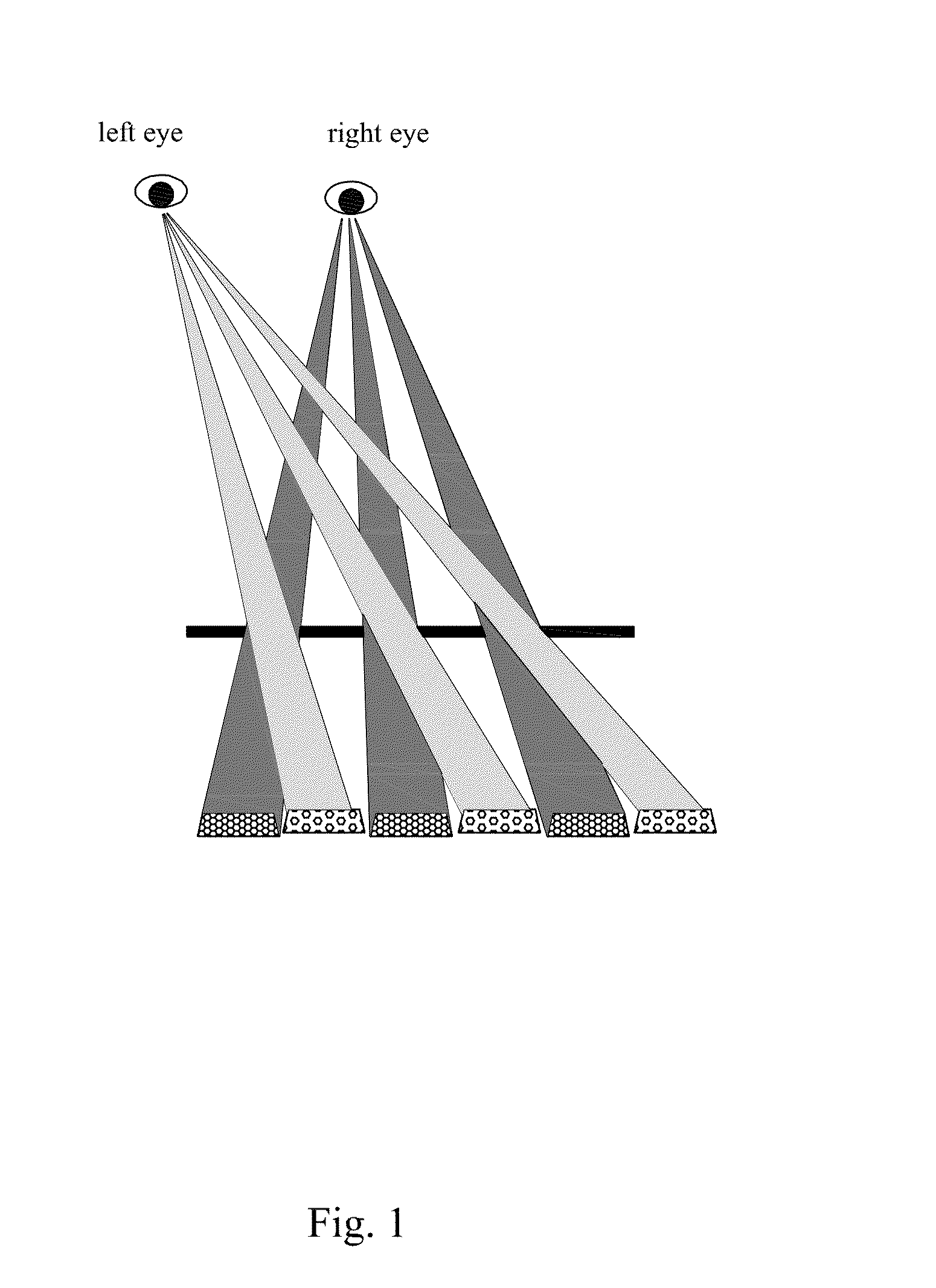
FIELD OF THE INVENTION[0001]The present invention relates to a field of 3-D displaying technology, and more particularly, to a 3-D displaying panel having depth-of-field effect and a displaying method thereof.DESCRIPTION OF PRIOR ART[0002]3D display technology has become the main stream of the display field. With the 3D display technology, a picture or image can be made to become a three-dimensional lifelike images which are no longer confined to the plane of the screen, as if the images walk out of the screen, thereby providing the audience an immersive feeling. Currently, the 3D display technology is generally used to implement the principle of binocular disparity, i.e. two parallax images (i.e., left and right parallax images) displayed on a two-dimensional display. Then, with a technique by using the viewer's left and right eyes, respectively, the view can see the 3-D effect by seeing the left or right parallax images on a two-dimensional display each time.[0003]3D display techn...

Claims


Application Information

Patent Timeline
IPC IPC(8): H01L27/32G09G3/32G09G3/00G02B30/30
CPCH01L27/326G09G3/3225G09G3/003G02B30/30H10K59/121H10K59/879H04N13/32G02B30/27H10K50/85
Inventor XU, XIANGYANG
Owner TCL CHINA STAR OPTOELECTRONICS TECH CO LTD
Learn More