Method And System For A Silicon-Based Optical Phase Modulator With High Modal Overlap

a phase modulator and silicon-based technology, applied in the field of semiconductor photonics, can solve the problems of cable bulk penalties, large power requirements, complex structure, etc., and achieve the effects of small improvement in reach, limited scalability, and limited scalability

Active Publication Date: 2015-12-31
CISCO TECH INC
View PDF17 Cites 15 Cited by
  • Summary
  • Abstract
  • Description
  • Claims
  • Application Information

AI Technical Summary

Benefits of technology

[0004]Further limitations and disadvantages of conventional and traditional approaches will become apparent to one of skill in the art, through comparison of such systems with the present disclosure as set forth in the remainder of the present application with reference to the drawings.

Problems solved by technology

They can be mitigated to some extent with equalization, coding, and shielding, but these techniques require considerable power, complexity, and cable bulk penalties while offering only modest improvements in reach and very limited scalability.

Method used


Image

  • Method And System For A Silicon-Based Optical Phase Modulator With High Modal Overlap
  • Method And System For A Silicon-Based Optical Phase Modulator With High Modal Overlap
  • Method And System For A Silicon-Based Optical Phase Modulator With High Modal Overlap

Examples


Embodiment Construction

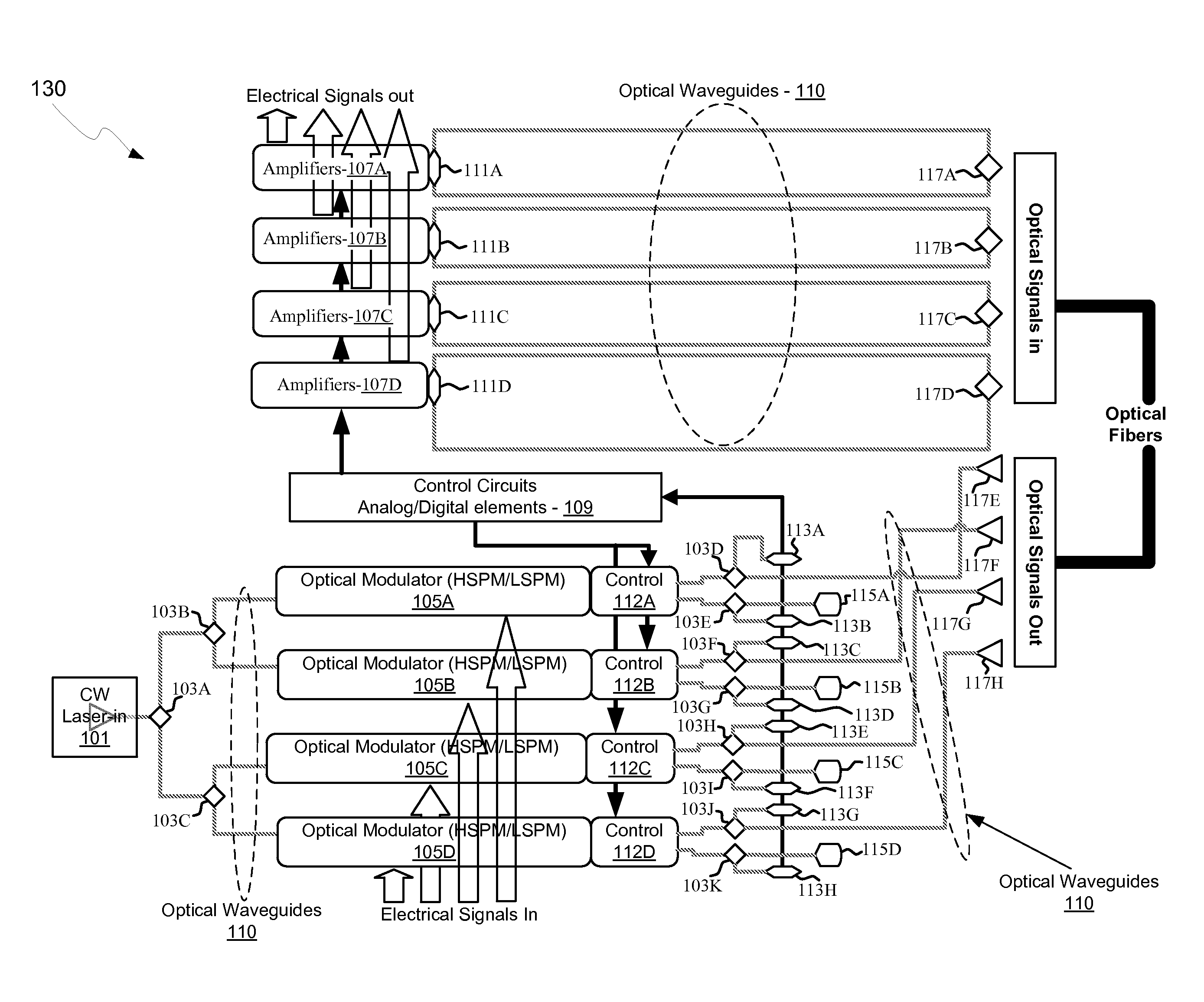
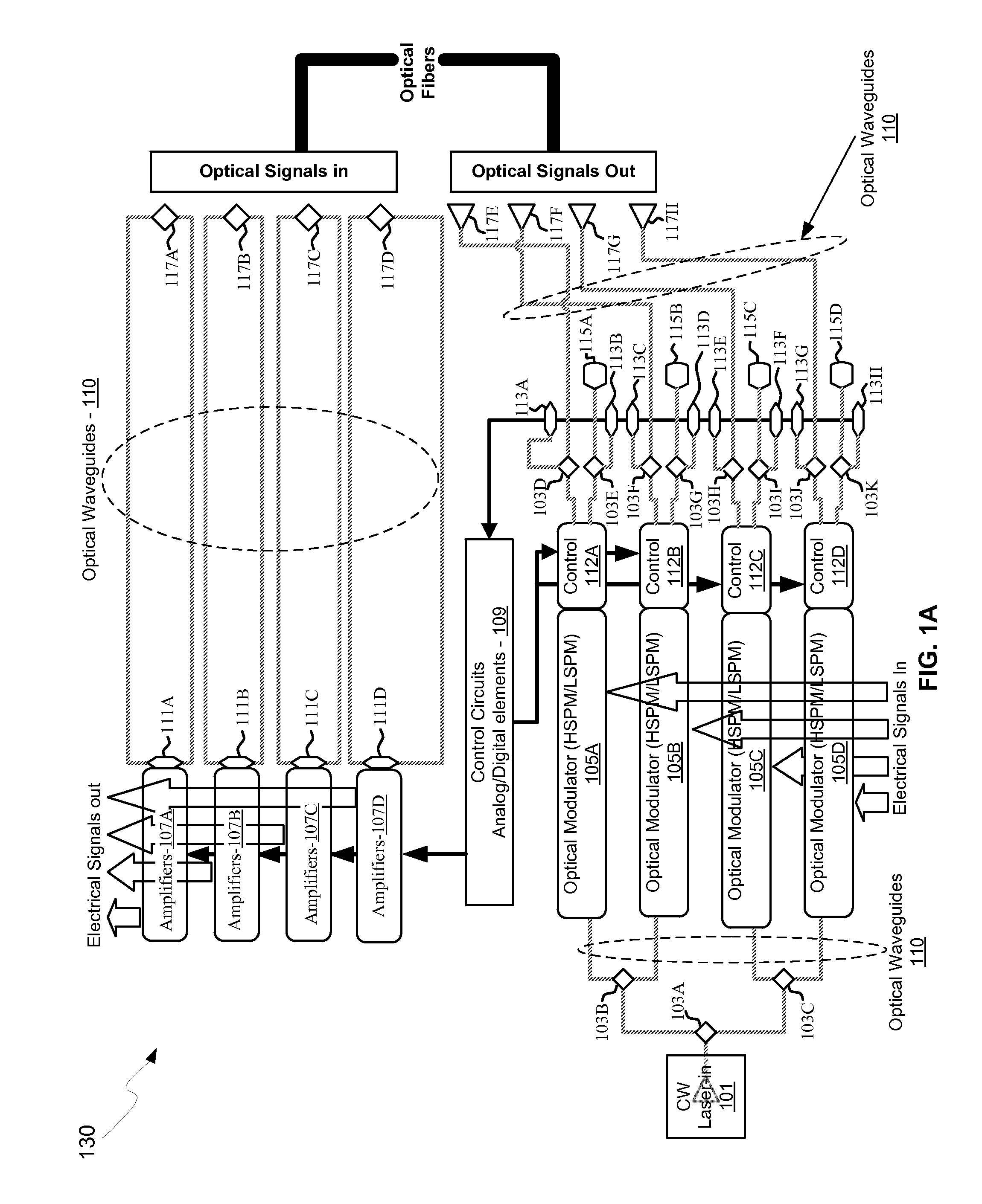
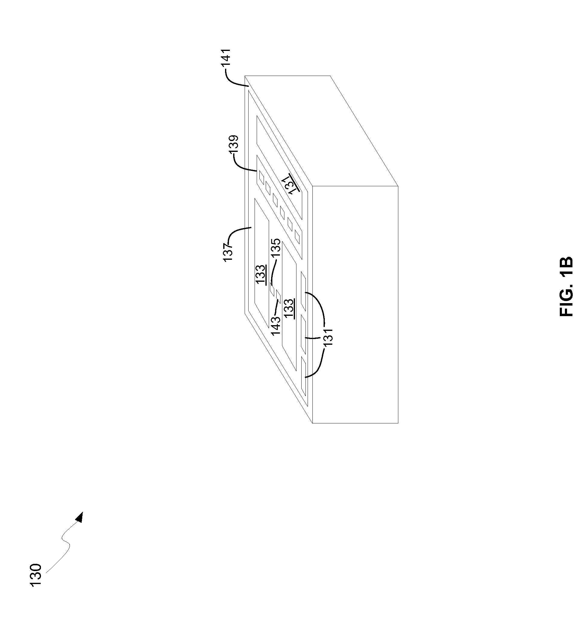
[0013]Certain aspects of the disclosure may be found in a method and system for a silicon-based optical phase modulator with high modal overlap. Exemplary aspects of the disclosure may comprise, in an optical modulator having a rib waveguide in which a cross-shaped depletion region separates four alternately doped sections: receiving an optical signal at one end of the optical modulator, modulating the received optical signal by applying a modulating voltage to the optical modulator, and communicating a modulated optical signal out of an opposite end of the optical modulator. The optical modulator may be in a silicon photonically-enabled integrated circuit. The silicon photonically-enabled integrated circuit may be in a complementary-metal oxide semiconductor (CMOS) die. An optical mode from the received optical signal may be centered on the cross-shaped depletion region. The four alternately doped sections may comprise: a shallow depth p-region, a shallow depth n-region, a deep p-r...


PUM


Abstract

Methods and systems for a silicon-based optical phase modulator with high modal overlap are disclosed and may include, in an optical modulator having a rib waveguide in which a cross-shaped depletion region separates four alternately doped sections: receiving an optical signal at one end of the optical modulator, modulating the received optical signal by applying a modulating voltage, and communicating a modulated optical signal out of an opposite end of the modulator. The modulator may be in a silicon photonically-enabled integrated circuit which may be in a complementary-metal oxide semiconductor (CMOS) die. An optical mode may be centered on the cross-shaped depletion region. The four alternately doped sections may include: a shallow depth p-region, a shallow depth n-region, a deep p-region, and a deep n-region. The shallow depth p-region may be electrically coupled to the deep p-region periodically along the length of the modulator.

Description

CROSS-REFERENCE TO RELATED APPLICATIONS / INCORPORATION BY REFERENCE[0001]This application claims priority to and the benefit of U.S. Provisional Application 61 / 998,386 filed on Jun. 26, 2014, which is hereby incorporated herein by reference in its entirety.FIELD[0002]Certain embodiments of the disclosure relate to semiconductor photonics. More specifically, certain embodiments of the disclosure relate to a method and system for a silicon-based optical phase modulator with high modal overlap.BACKGROUND[0003]As data networks scale to meet ever-increasing bandwidth requirements, the shortcomings of copper data channels are becoming apparent. Signal attenuation and crosstalk due to radiated electromagnetic energy are the main impediments encountered by designers of such systems. They can be mitigated to some extent with equalization, coding, and shielding, but these techniques require considerable power, complexity, and cable bulk penalties while offering only modest improvements in reac...

Claims


Application Information

Patent Timeline
Patent Type & Authority Applications(United States)
IPC IPC(8): H04B10/548H04B10/2581H04B10/50
CPCG02F1/025H04B10/548
Inventor SAHNI, SUBALHON, KAM-YANMEKIS, ATTILAMASINI, GIANLORENZOVERSLEGERS, LIEVEN
Owner CISCO TECH INC
Why Eureka
Try Eureka