Chip spacing maintaining apparatus

a technology of maintaining apparatus and chips, which is applied in the direction of metal working apparatus, printed circuit assembling, manufacturing tools, etc., can solve problems such as chips contamination, and achieve the effect of suppressing chips contaminated with volatile components of expand sheets and increasing spacing

Active Publication Date: 2016-01-07
DISCO CORP
View PDF3 Cites 54 Cited by
  • Summary
  • Abstract
  • Description
  • Claims
  • Application Information

AI Technical Summary

Benefits of technology

[0010]The chip spacing maintaining apparatus according to the present invention includes the air layer forming means for forming an air layer above the workpiece as described above. Accordingly, the deposition of the volatile components of the expand sheet volatilized by the heat of the far-infrared radiation can be suppressed by the air layer. As a result, the contamination of the chips with the volatile components of the expand sheet can be suppressed in maintaining the increased spacing between the chips.

Problems solved by technology

However, the above method of maintaining the spacing between the chips has a problem such that the volatile components of the expand sheet volatilized by the heating may be deposited to the chips, causing the contamination of the chips.

Method used


Image

  • Chip spacing maintaining apparatus
  • Chip spacing maintaining apparatus
  • Chip spacing maintaining apparatus

Examples


Embodiment Construction

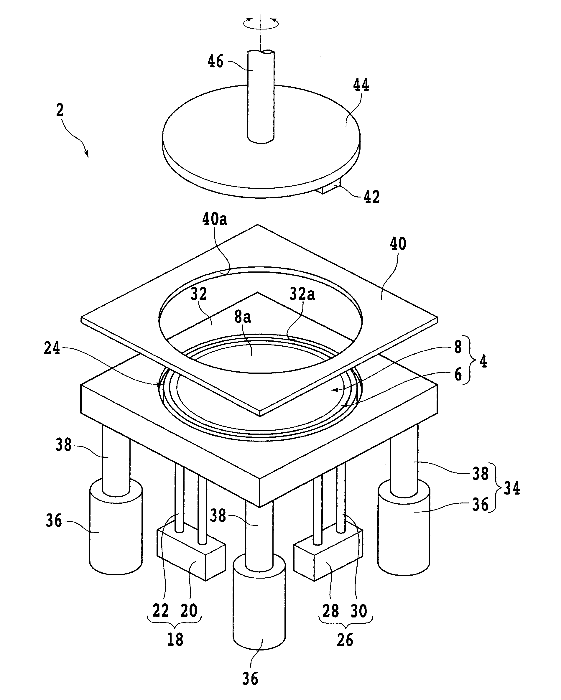
[0019]A preferred embodiment of the present invention will now be described with reference to the attached drawings. FIG. 1 is a perspective view schematically showing a workpiece to be processed by a chip spacing maintaining apparatus according to this preferred embodiment. As shown in FIG. 1, a workpiece 11 is a substantially circular platelike workpiece (wafer) formed of silicon, for example. The workpiece 11 has a front side 11a and a back side 11b. The front side 11a of the workpiece 11 is composed of a central device area 13 and a peripheral marginal area 15 surrounding the device area 13. The device area 13 is partitioned into a plurality of regions by a plurality of crossing streets (division lines) 17. A plurality of devices 19 such as ICs are formed in these plural regions, respectively. The outer circumference of the workpiece 11 is chamfered to have a round shape in cross section.

[0020]A modified layer 21 as a division start point is formed inside the workpiece 11 along ...


PUM


Abstract

A chip spacing maintaining apparatus for maintaining the spacing between any adjacent ones of a plurality of chips obtained by dividing a workpiece attached to an expand sheet, the expand sheet being supported at its peripheral portion to an annular frame is provided. The chip spacing maintaining apparatus includes a far-infrared radiation applying unit for applying far-infrared radiation toward the expand sheet expanded in a target area between the outer circumference of the workpiece and the inner circumference of the annular frame, thereby shrinking the expand sheet in the target area, and an air layer forming unit provided adjacent to the far-infrared radiation applying unit, the air layer forming unit having a nozzle hole for discharging a gas toward the workpiece in applying the far-infrared radiation from the far-infrared radiation applying unit toward the expand sheet, thereby forming an air layer above the workpiece.

Description

BACKGROUND OF THE INVENTION[0001]1. Field of the Invention[0002]The present invention relates to a chip spacing maintaining apparatus for maintaining the spacing between chips formed by expanding an expand sheet.[0003]2. Description of the Related Art[0004]In compact and lightweight electronic equipment represented by a mobile phone, a device chip having a device such as an IC is an essential component. Such a device chip (which will be hereinafter referred to simply as chip) is manufactured by using wafer formed of silicon, for example, partitioning the front side of the wafer with a plurality of division lines called streets to thereby form a plurality of separate regions, forming a device in each separate region, and dividing the wafer along each street.[0005]In recent years, there has been put into practical use a dividing method including the steps of forming a modified layer as a division start point inside the wafer along each street and next applying an external force to the...

Claims


Application Information

Patent Timeline
Patent Type & Authority Applications(United States)
IPC IPC(8): H05K3/30
CPCH05K3/30H01L21/68H01L21/78H01L21/67115H01L21/67132H01L21/6836H01L2221/68336
Inventor HATTORI, ATSUSHIUEKI, ATSUSHI
Owner DISCO CORP
Why Eureka
Try Eureka