Interleaved Delta-Sigma Modulator
- Summary
- Abstract
- Description
- Claims
- Application Information
AI Technical Summary
Benefits of technology
Problems solved by technology
Method used
Image
Examples
Embodiment Construction
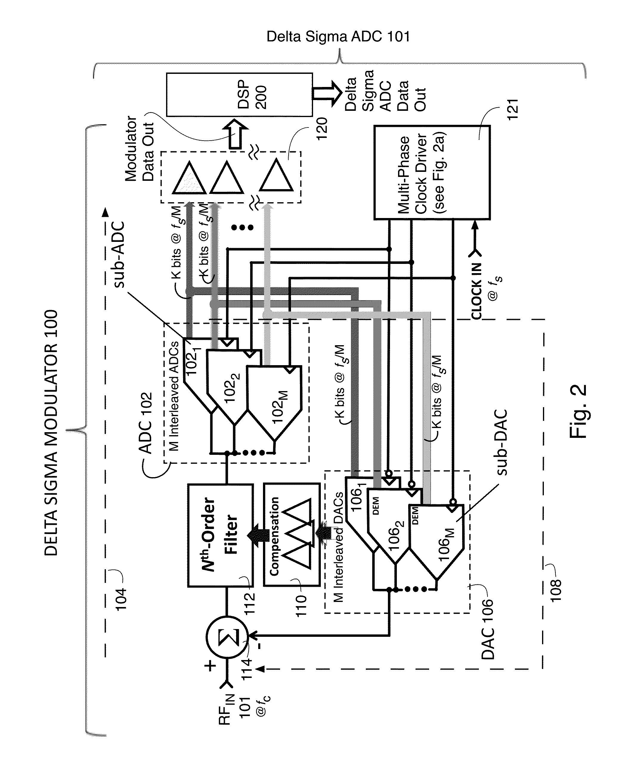
[0032]A block diagram of the ΔΣ modulator 100 architecture of the present invention is illustrated by FIG. 2. The block diagram is shown for the most generic case: an Nth Order filter, an M time-wise interleaving factor, and K-bits in the quantizers of the depicted ADCs 1021-102M and the depicted DACs 1061-106M with a modulator clock rate of fs. The architecture presented is different from a conventional continuous time ΔΣ modulator in that there is a bank 102 of interleaved Analog to Digital Converters (ADCs) 1021-102M in a forward path 104 and a bank 106 having an equal number of interleaved Digital to Analog Converters (DACs) 1061-106M in a feedback path 108. The input signal RFIN is applied to a summing block 114 with the feedback path being subtracted at that summing block 116. The analog input characteristics (amplitude, frequency) of the RFIN signal are encoded into a digital pulse stream which is applied to a DSP 200 which decimates the pulse string and when connected to the...
PUM
 Abstract
Description
Claims
Application Information


