
Through-hole layout structure, circuit board, and electronic assembly

Active Publication Date: 2016-01-21
VIA LABS INC
View PDF0 Cites 3 Cited by
  • Summary
  • Abstract
  • Description
  • Claims
  • Application Information

AI Technical Summary

Benefits of technology

The invention is about a way to reduce interference when signals are sent through a circuit board. The invention adds a ground through-hole to make sure that differential through-holes have a reference point, which helps to maintain the signal's symmetry and reduce interference. This makes the circuit board more reliable and efficient for transmitting signals.

Problems solved by technology

However, issues of electromagnetic interference (EMI) / radio frequency interference (RFI) may occur at a frequency of about 2.5 GHz.
Therefore, an apparatus (such as the wireless module of a wireless mouse) at an operating frequency of about 2.5 GHz may fail due to interference from the signal of USB 3.0.
When the differential transmission path is asymmetric, the differential signal may be converted to an undesired common mode noise, thereby causing the issue of RFI.

Method used


Image

  • Through-hole layout structure, circuit board, and electronic assembly
  • Through-hole layout structure, circuit board, and electronic assembly
  • Through-hole layout structure, circuit board, and electronic assembly

Examples


Embodiment Construction

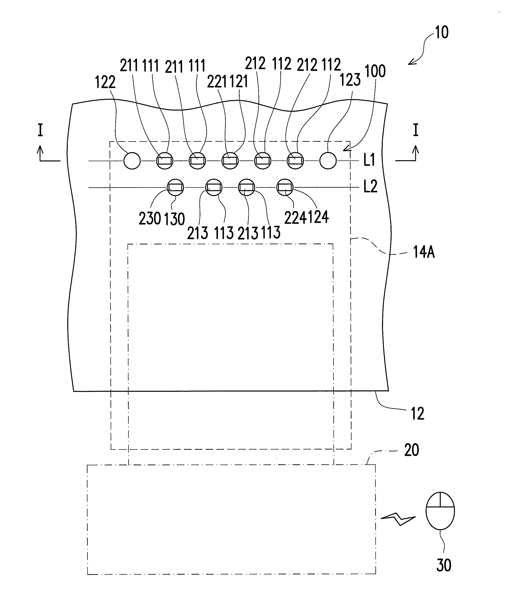
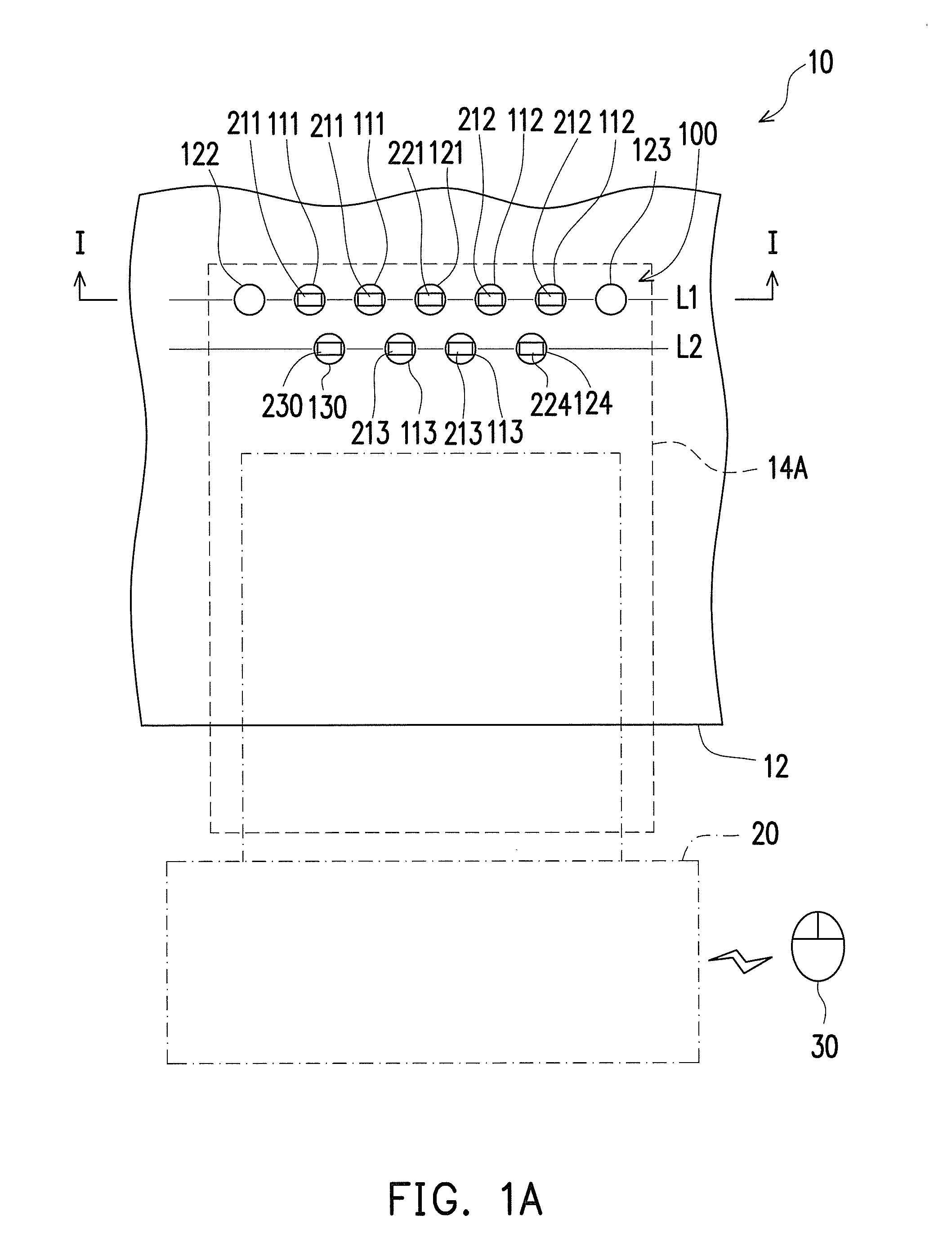
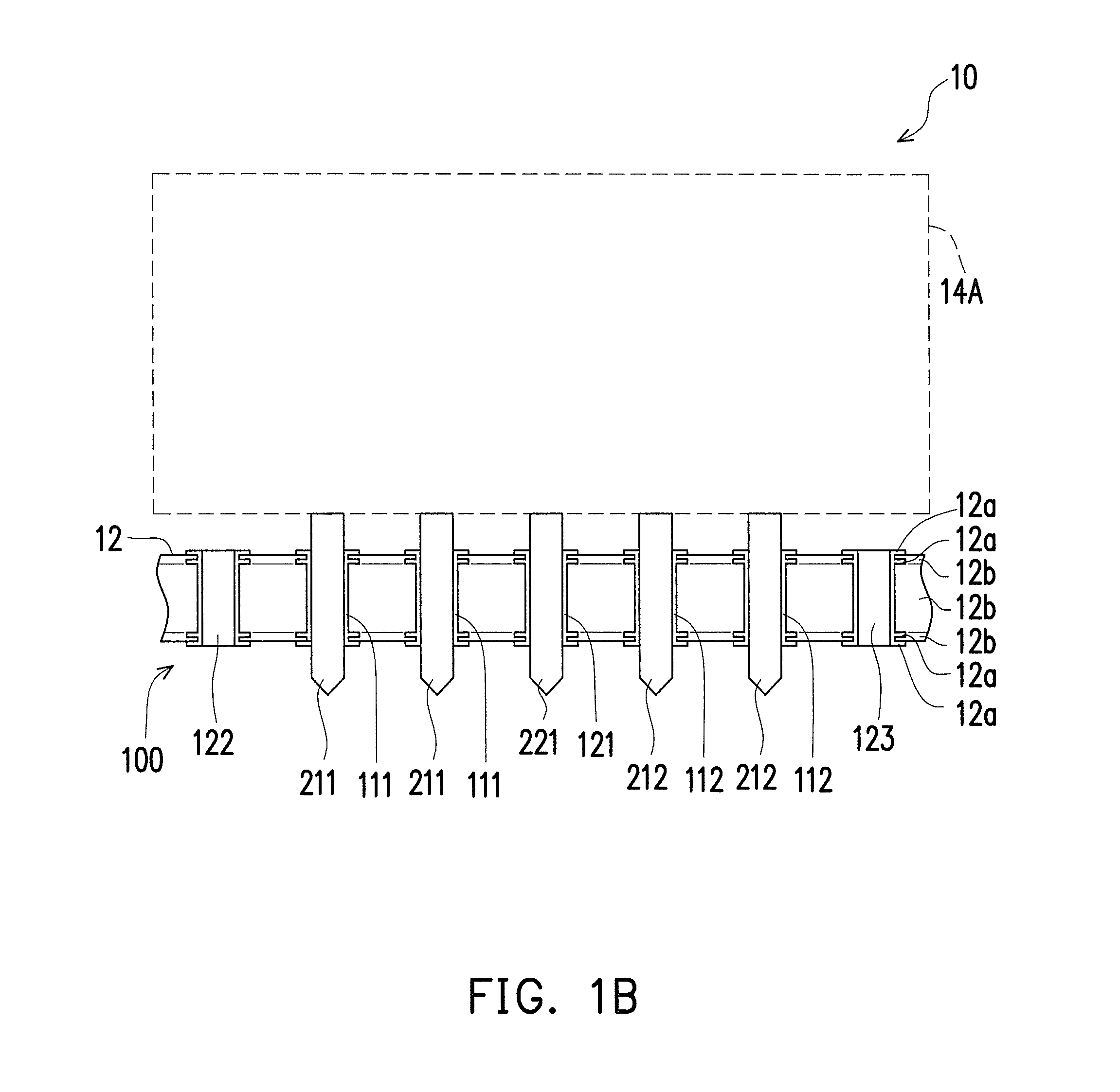
[0020]Referring to FIG. 1A and FIG. 1B, in the present embodiment, an electronic assembly 10 includes a circuit board 12 and an electrical connector 14A installed on the circuit board 12. A USB 3.0 or USB 3.1 chip (not shown) can further be installed on the circuit board 12, and the USB 3.0 or USB 3.1 chip is electrically connected to the electrical connector 14A via the circuit board 12. The circuit board 12 includes a plurality of patterned conductive layers 12a and a plurality of dielectric layers 12b, and the patterned conductive layers 12a and the dielectric layers 12b are alternately stacked, as shown in FIG. 1B. To install the electrical connector 14A on the circuit board 12, the circuit board 12 includes a plurality of through-holes, and a plurality of pins of the electrical connector 14A are respectively plugged into the through-holes.

[0021]In the present embodiment, the electrical connector 14A is a standard A-type receptacle connector of USB 3.0 or USB 3.1. Therefore, the...


PUM


Abstract

A through-hole layout structure is suitable for a circuit board. The through-hole layout structure includes a pair of first differential through-holes, a pair of second differential through-holes, a first ground through-hole, a second ground through-hole, and a third ground through-hole, which are all arranged on a first line.The first ground through-hole is located between the pair of first differential through-holes and the pair of second differential through-holes. The pair of first differential through-holes is located between the first ground through-hole and the second ground through-hole. The pair of second differential through-holes is located between the first ground through-hole and the third ground through-hole.

Description

CROSS-REFERENCE TO RELATED APPLICATION[0001]This application claims the priority benefits of U.S. provisional application Ser. No. 62 / 025,992, filed on Jul. 17, 2014 and Taiwan application serial no. 103131781, filed on Sep. 15, 2014. The entirety of each of the above-mentioned patent applications is hereby incorporated by reference herein and made a part of this specification.BACKGROUND OF THE INVENTION[0002]1. Field of the Invention[0003]The invention relates to a circuit board, and more particularly, to a through-hole layout structure suitable for a circuit board and used to reduce signal interference, and a circuit board and an electronic assembly adopting the through-hole layout structure.[0004]2. Description of Related Art[0005]The application of the current USB 3.0 is relatively widespread. However, issues of electromagnetic interference (EMI) / radio frequency interference (RFI) may occur at a frequency of about 2.5 GHz. The reason is, USB 3.0 has a data rate of 5 Gbps and the...

Claims


Application Information

Patent Timeline
IPC IPC(8): H05K1/02H01P3/08H05K1/11
CPCH05K1/0216H05K1/115H05K2201/10189H05K2201/042H01P3/08H05K1/0222H05K1/182H05K1/0245
Inventor LEE, SHENG-YUAN
Owner VIA LABS INC
Learn More