Phase-shift blankmask and photomask

a phase-shift and blanking technology, applied in the field of phase-shift blanking masks and photomasks, can solve the problems of high semiconductor microfabrication process technology, defect in pattern, and the inability to meet the optical properties of light-shielding films, etc., and achieve the effect of improving the etching speed

Active Publication Date: 2016-02-25
S & S TECH
View PDF0 Cites 18 Cited by
  • Summary
  • Abstract
  • Description
  • Claims
  • Application Information

AI Technical Summary

Benefits of technology

[0010]The present invention is directed to a phase-shift blankmask having a light-shielding film which not only secures a light-shielding effect but also has an improved etching speed, and a photomask using the same.
[0011]Further, the present invention is directed to a phase-shift blankmask having a light-shielding film which has not only an improved etching speed but also a low sheet resistance, and a photomask using the same.
[0012]In addition, the present invention is directed to a phase-shift blankmask in which a resist film is thinly formed to prevent a resist pattern from being damaged, and a fine pattern is achieved to secure a high pattern accuracy, and a photomask using the same.

Problems solved by technology

Today, as a need for a fine circuit pattern has been accompanied by high integration of large-scale integrated circuits (ICs), high semiconductor microfabrication process technology has emerged as a very important issue.
As the resist film is thick, the resist film has a deviation in a critical dimension due to a loading effect while forming a pattern, thereby causing a defect in the pattern.
However, a problem arises in that the reduced thickness of the light-shielding film cannot satisfy required optical properties, e.g., optical density, reflectivity, etc.
However, the light-shielding film containing oxygen (O) has a problem of increasing sheet resistance under a certain condition due to a composition ratio, a fabrication process, etc.

Method used


Image

  • Phase-shift blankmask and photomask
  • Phase-shift blankmask and photomask
  • Phase-shift blankmask and photomask

Examples


embodiments

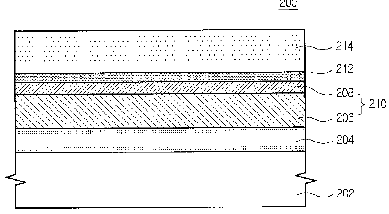
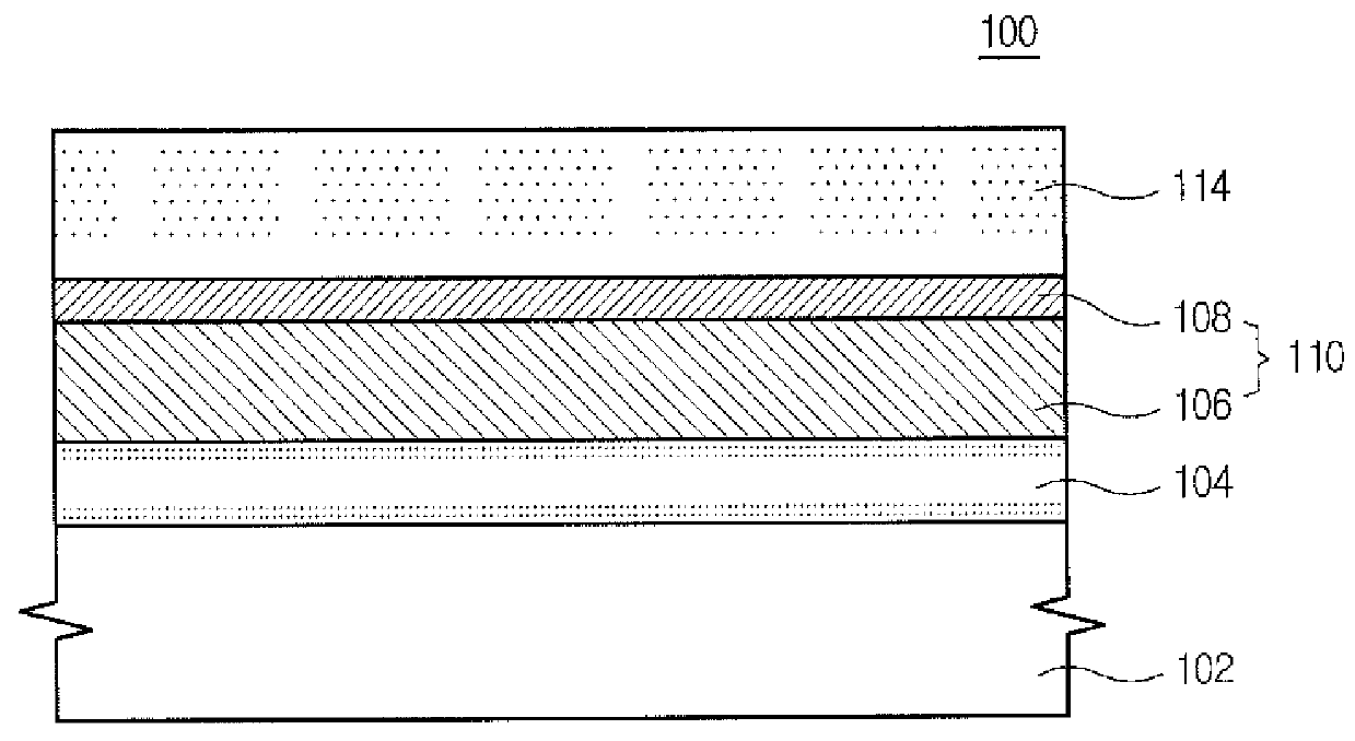
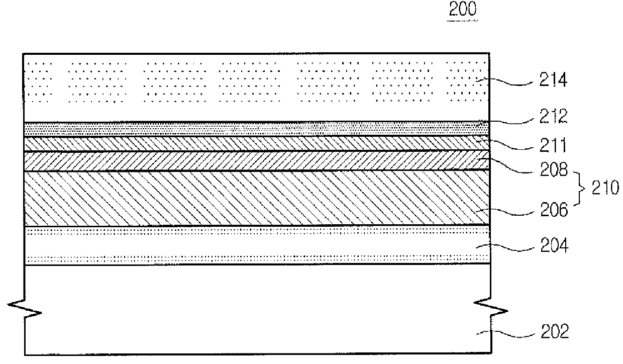
[0068]Evaluation I of Properties Based on Materials for Light-Shielding Film

[0069]To specify materials and their contents for the light-shielding film provided in the phase-shift blankmask according to an embodiment of the present invention, chrome (Cr) compounds having different composition ratios were evaluated with respect to the etching speed and film properties.

[0070]The light-shielding film was grown on a transparent substrate by a direct current (DC) magnetron sputtering apparatus with a chrome (Cr) target.

[0071]Table 1 shows that an etching speed of a metal film containing chrome (Cr) as major element is varied depending on the kinds of light element contained therein.

TABLE 1Materials for filmsCrCCrCrNCrONProcess gasAr:CH4ArAr:N2Ar:N2:NO(sccm)(5:3)(8)(5:3)(5:3:3)Process power0.70.70.70.7(KW)Etching speed0.40.91.31.8(Å / sec)

[0072]Referring to Table 1, the etching speed of the chrome (Cr) compounds was high in order of chrome carbide (CrC), chrome (Cr), chrome nitride (CrN) and...


PUM

PropertyMeasurementUnit
surface reflectivityaaaaaaaaaa
optical densityaaaaaaaaaa
flatnessaaaaaaaaaa

Abstract

Disclosed is a phase-shift blankmask, in which a light-shielding film includes a metal compound and having a structure of a multi-layer film or a continuous film, which includes a first light-shielding layer and a second light-shielding layer. The second light-shielding layer has higher optical density at an exposure wavelength per unit thickness (Å) than the first light-shielding layer. The first light-shielding layer occupies 70% to 90% of the whole thickness of the light-shielding film. With this, the blankmask secures a light-shielding effect, has an improved etching speed, and makes a resist film thinner, thereby achieving a fine pattern.

Description

CROSS-REFERENCE TO RELATED APPLICATION[0001]This application claims priority to and the benefit of Korean Patent Application Nos. 10-2014-0110771 filed on Aug. 25, 2014, 10-2015-0038683 filed on Mar. 20, 2015 and 10-2015-0048095 filed on Apr. 6, 2015, the disclosure of which is incorporated herein by reference in its entirety.BACKGROUND[0002]1. Field of the Invention[0003]The present invention relates to a phase-shift blankmask and a photomask, and more particularly to a phase-shift blankmask and a photomask which can achieve a fine pattern of not greater than 32 nm, preferably not greater than 14 nm, and more preferably not greater than 10 nm.[0004]2. Discussion of Related Art[0005]Today, as a need for a fine circuit pattern has been accompanied by high integration of large-scale integrated circuits (ICs), high semiconductor microfabrication process technology has emerged as a very important issue.[0006]To this end, lithography technology has been developed up to a binary intensity...

Claims


Application Information

Patent Timeline
Patent Type & Authority Applications(United States)
IPC IPC(8): G03F1/26
CPCG03F1/26
Inventor NAM, KEE-SOOSHIN, CHEOLYANG, CHUL-KYULEE, JONG-HWACHOI, MIN-KIKIM, CHANG-JUNJANG, KYU-JIN
Owner S & S TECH
Why Eureka
Try Eureka