Method for fabricating semiconductor device improving the process speed

Inactive Publication Date: 2016-02-25
SAMSUNG ELECTRONICS CO LTD
View PDF1 Cites 2 Cited by
  • Summary
  • Abstract
  • Description
  • Claims
  • Application Information

AI Technical Summary

Benefits of technology

The patent text is talking about a new method for making semiconductor devices that makes the process faster.

Problems solved by technology

As the result, the transformed crystals act as stressors, thereby affecting the lattice structure of the channel region and ultimately increasing the charge carrier mobility.

Method used


Image

  • Method for fabricating semiconductor device improving the process speed
  • Method for fabricating semiconductor device improving the process speed
  • Method for fabricating semiconductor device improving the process speed

Examples


first embodiment

[0027]Hereinafter, a method for fabricating a semiconductor device according to the present inventive concepts will be described with reference to FIGS. 1 to 13.

[0028]FIGS. 1 to 13 illustrate intermediate process steps in a method for fabricating a semiconductor device according to a first embodiment of the present inventive concepts. Specifically, FIGS. 5 and 7 are cross-sectional views taken along the line B-B′ of FIGS. 4 and 6.

[0029]The method for fabricating the semiconductor device according to the first embodiment of the present inventive concepts may be a method for fabricating an NMOS transistor. Therefore, while a process for the method for fabricating the semiconductor device according to the first embodiment of the present inventive concepts is performed, a region other than an NMOS region (e.g., a PMOS region) may be covered by a mask.

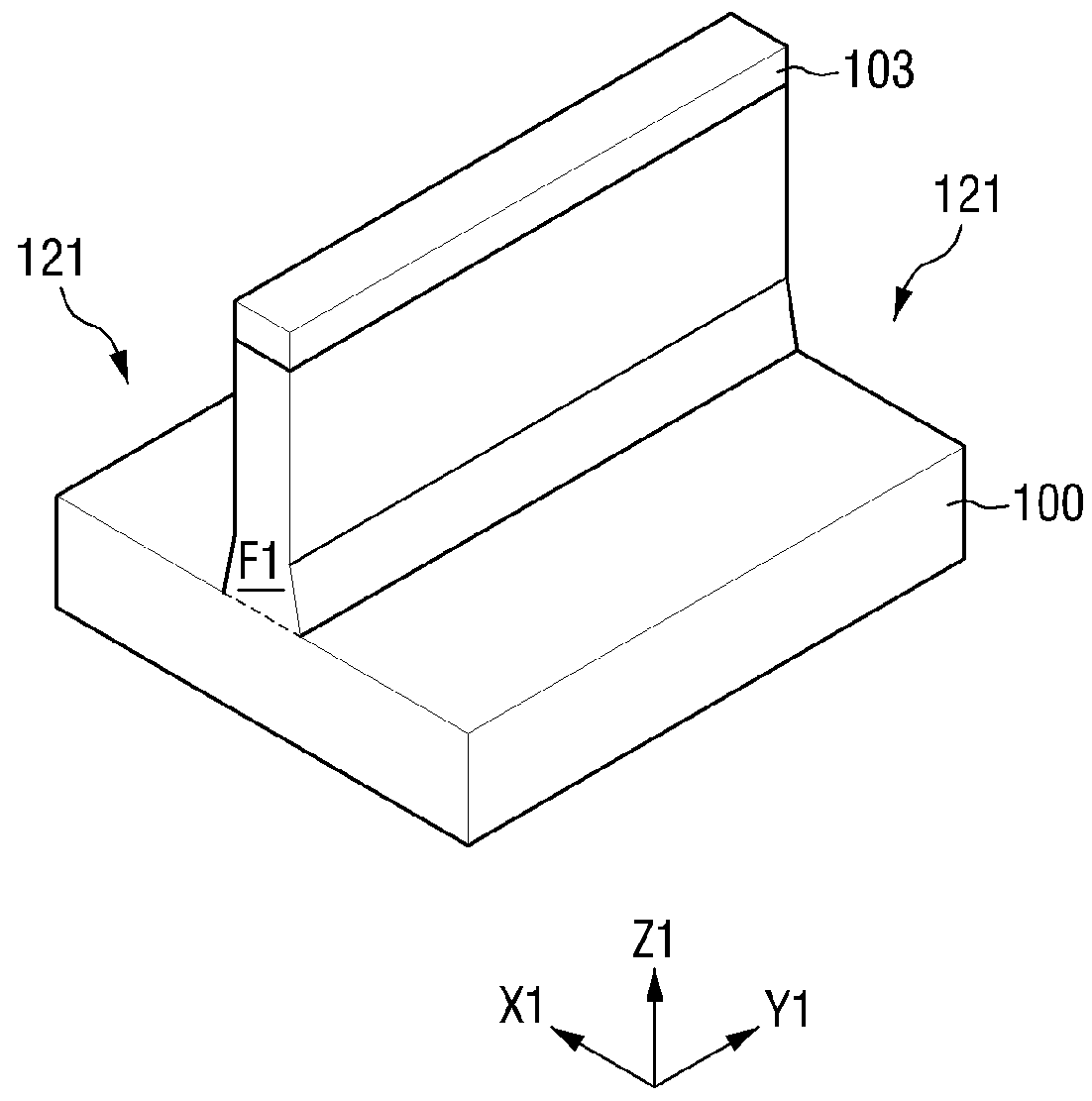
[0030]Referring to FIG. 1, a fin F1 is formed on a substrate 100.

[0031]In detail, a mask pattern 103 is formed on the substrate 100, follo...

second embodiment

[0069]FIG. 14 illustrates intermediate process steps in a method for fabricating a semiconductor device according to the present inventive concepts.

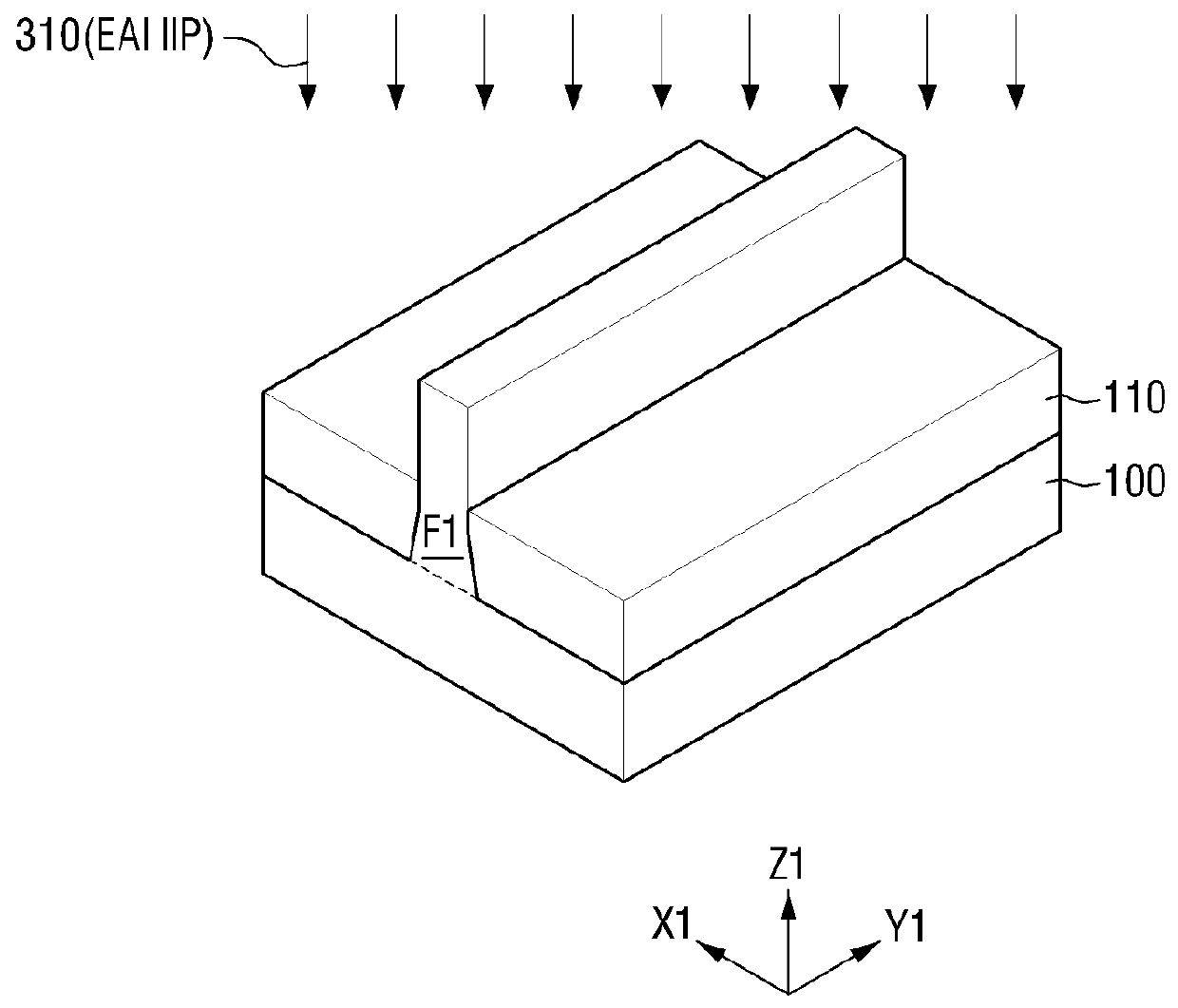
[0070]Referring to FIG. 14(a), a fin F1 is formed on a substrate 100.

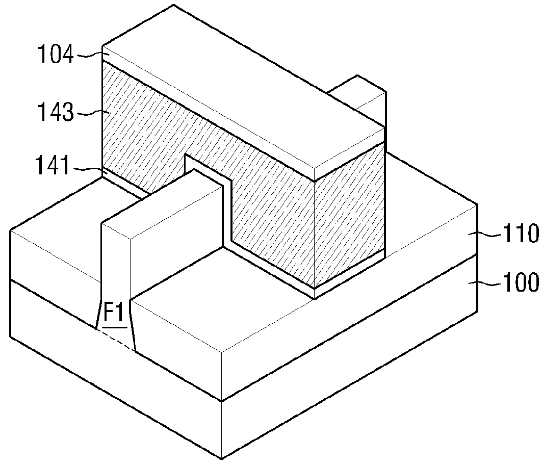
[0071]Referring to FIG. 14(b), a gate insulation layer 141 and a gate electrode 143, crossing the fin F1, are formed. Spacers 151 are formed on sidewalls of the gate electrode 143 and sidewalls of the fin F1.

[0072]Referring to FIG. 14(c), a pre-amorphization implantation (PAI) process is performed (371) to form an amorphized region 321.

[0073]Referring to FIG. 14(d), a first impurity, e.g., electrically active impurities (EAIs), is first ion-implanted into the fin F1 (372).

[0074]Referring to FIG. 14(e), a stress inducing layer 340 is formed on the substrate 100, the fin F1 and the gate electrode 143. In addition, before the forming of the stress inducing layer 340, a buffer layer 330 may be formed. The substrate 100 may be annealed to recrystallize the amorphized region ...

third embodiment

[0077]FIG. 15 illustrates intermediate process steps in a method for fabricating a semiconductor device according to the present inventive concepts.

[0078]Referring to FIG. 15(a), a fin F1 is formed on a substrate 100.

[0079]Referring to FIG. 15(b), a first impurity, e.g., electrically active impurities (EAIs), is first ion-implanted into the fin F1 (381).

[0080]Referring to FIG. 15(c), a gate insulation layer 141 and a gate electrode 143, crossing the fin F1, are formed. Spacers 151 are formed on sidewalls of the gate electrode 143 and sidewalls of the fin F1.

[0081]Referring to FIG. 15(d), a pre-amorphization implantation (PAI) process is performed (371) to form an amorphized region 321, and a third impurity, e.g., electrically active impurities (EAIs), is third ion-implanted into the fin F1 (382).

[0082]Here, the third impurity may be B, As, P, Sb, Si, Ge or combinations thereof. The third impurity may be different from the impurity used in the PAI process. The third impurity may impr...


PUM


Abstract

A method for fabricating a semiconductor device improving the process speed is provided. The method includes forming a fin on a substrate, forming a gate electrode on the fin, first ion-implanting a first impurity to amorphize a region including portions of the fin positioned at opposite sides of the gate electrode, forming a stress inducing layer on the substrate and the fin, and annealing the substrate to recrystallize the amorphized region, wherein after the forming of the fin and before the annealing, the method further includes second ion-implanting a second impurity different from the first impurity into the fin.

Description

CROSS-REFERENCE TO RELATED APPLICATION[0001]This application claims priority from Korean Patent Application No. 10-2014-0109095 filed on Aug. 21, 2014 in the Korean Intellectual Property Office, and all the benefits accruing therefrom under 35 U.S.C. 119, the contents of which in its entirety are herein incorporated by reference.BACKGROUND[0002]1. Field of the Inventive Concepts[0003]The present inventive concepts relates to a method for fabricating a semiconductor device improving the process speed.[0004]2. Description of the Related Art[0005]In order to improve performance of a metal oxide semiconductor (MOS) transistor, conductivity of a channel region of the MOS transistor may be increased. For example, the charge carrier mobility may be increased by altering a lattice structure of the channel region, thereby increasing the conductivity of the channel region of the MOS transistor.[0006]The lattice structure of the channel region may be altered by generating a stressor near the c...

Claims


Application Information

Patent Timeline
IPC IPC(8): H01L29/66H01L21/265
CPCH01L21/265H01L29/66795H01L29/7847H01L29/7848
Inventor CHIN, HOCK-CHUNSON, NAK-JINLEE, SANG-HYEON
Owner SAMSUNG ELECTRONICS CO LTD
Why Eureka
Try Eureka